Surface-enhanced raman scattering substrate and manufacturing method thereof

a technology of raman scattering and surface enhancement, which is applied in the field of surface enhancement of raman scattering substrate and the manufacturing method thereof, can solve the problems of limiting the application of sers in the related field, high cost and inability to reduce, and high cost, and achieves high sensitivity sers and high density metal nanoparticles. , the effect of wide application

Active Publication Date: 2016-12-13
NAT TAIWAN UNIV
View PDF7 Cites 0 Cited by
  • Summary
  • Abstract
  • Description
  • Claims
  • Application Information

AI Technical Summary

Benefits of technology

[0006]The disclosed example is to provide an ecofriendly, wide application, high sensitivity SERS substrate with high density metal nanoparticle. The production method of this substrate not only is fast and easy for producing, but also can be done efficiently.

Problems solved by technology

Those processing procedures are complicated, and the costs are high and not reducible, thus limiting the application of the SERS in the related field and the SERS only being used in the laboratory.

Method used


Image

  • Surface-enhanced raman scattering substrate and manufacturing method thereof
  • Surface-enhanced raman scattering substrate and manufacturing method thereof
  • Surface-enhanced raman scattering substrate and manufacturing method thereof

Examples


Embodiment Construction

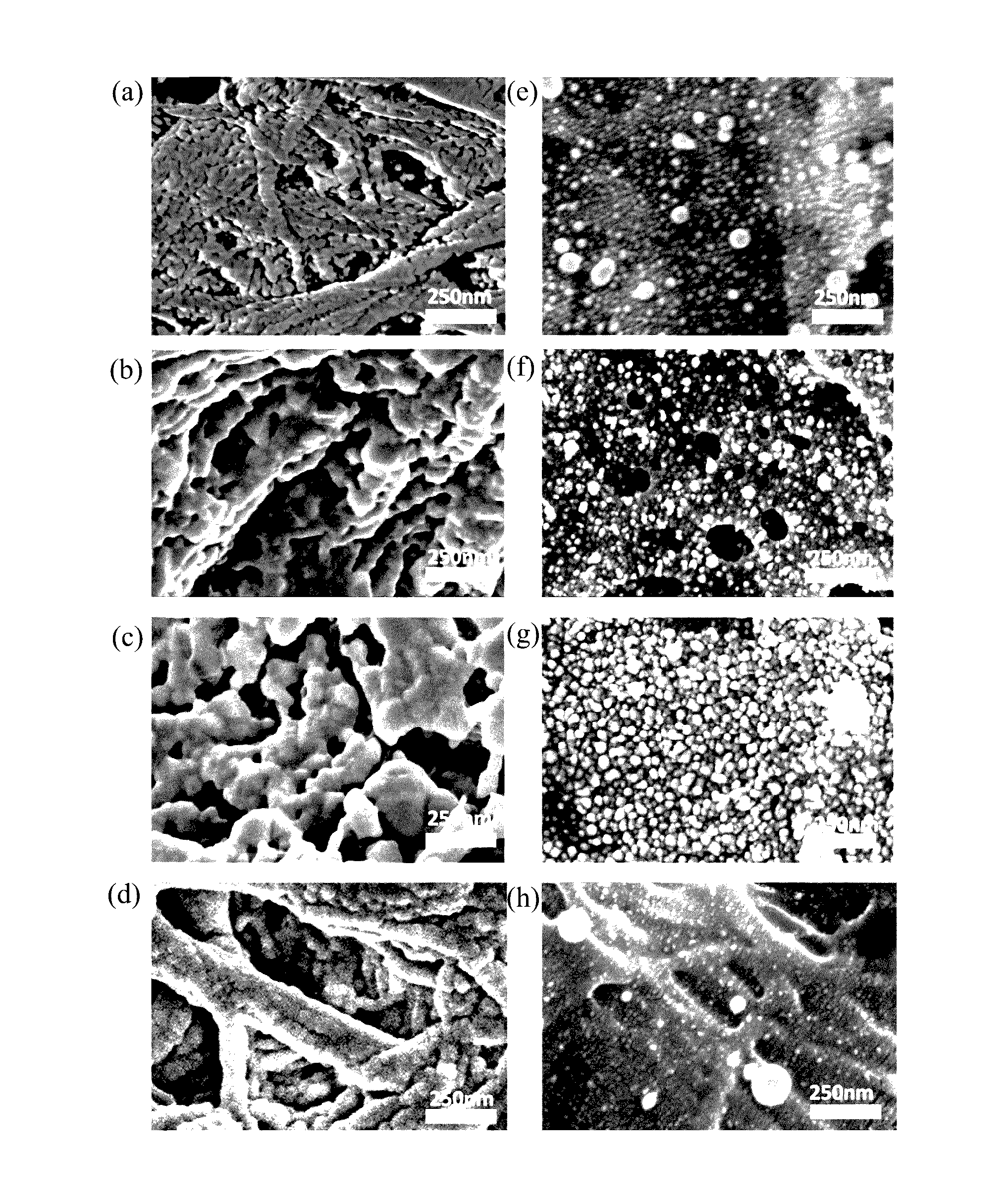
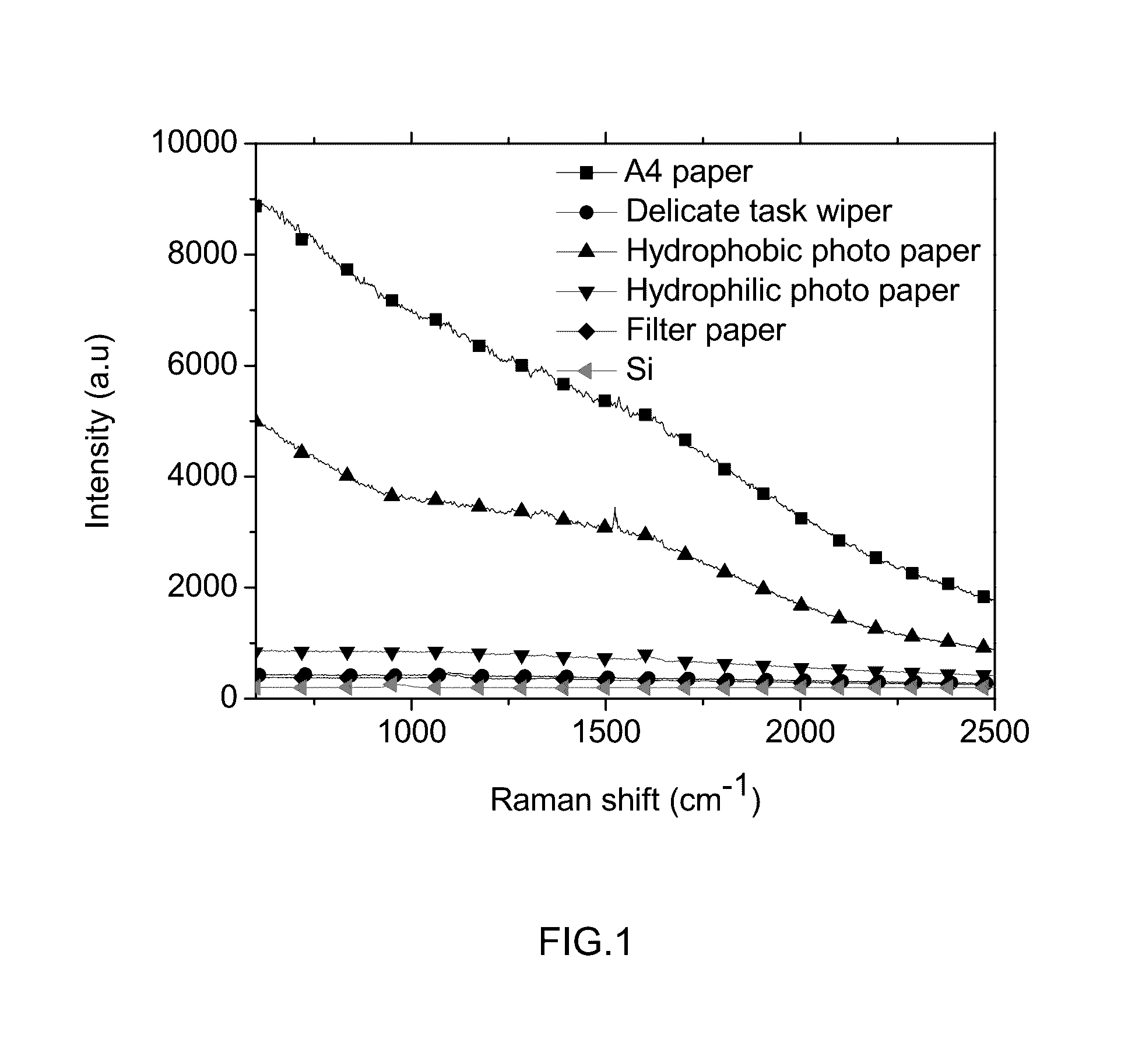
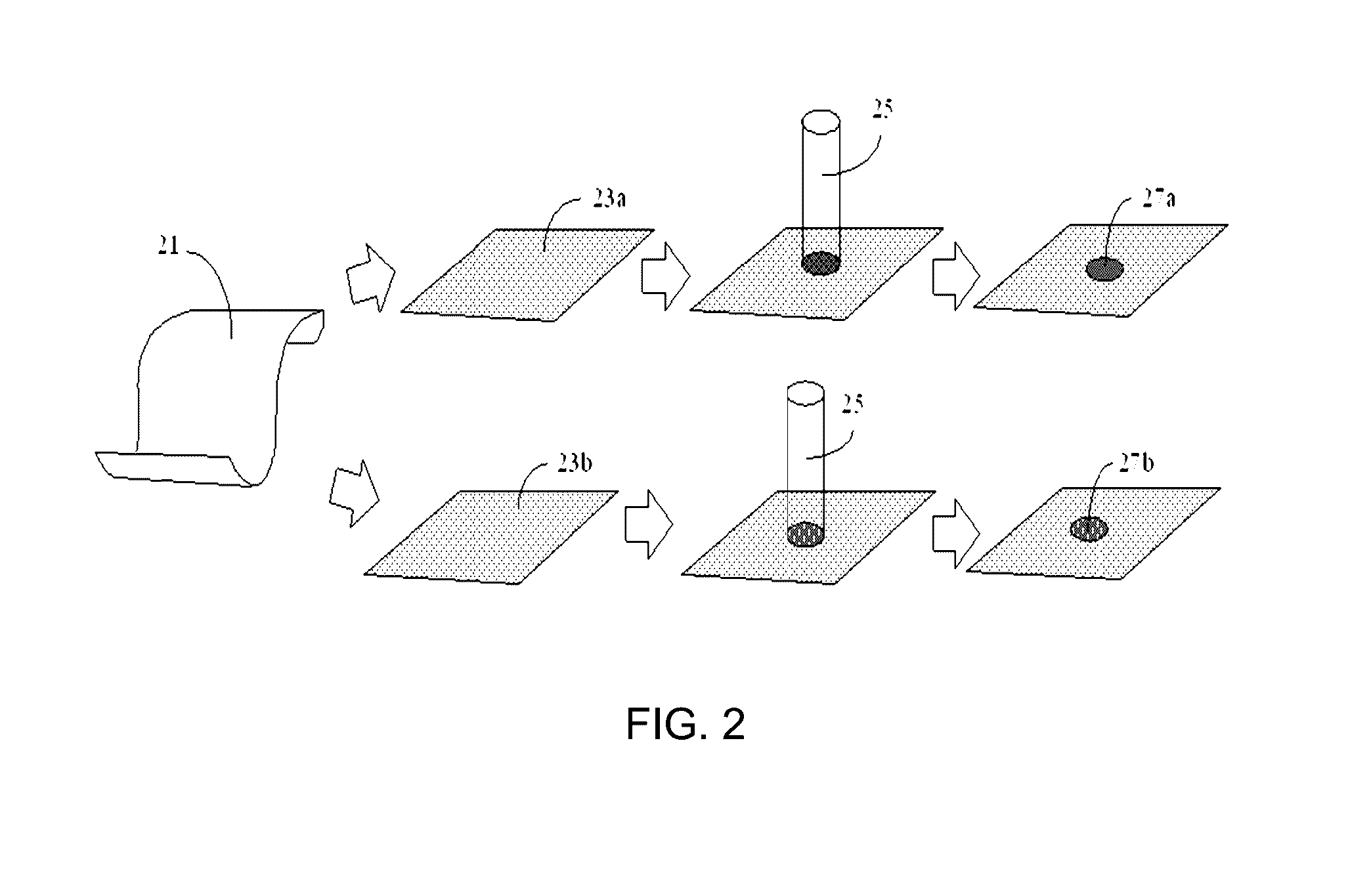
[0029]The disclosed example uses low thermal conductivity base to restrict the laser energy to the metal thin film, only a small parts of the energy will be conducted to the low thermal conductivity base, thereby enhancing the light-heat conversion efficiency, and most of the thermal energy transformed from the laser will be conducted to the metal thin film. Paper or oxide base (such as glass) can both be the low thermal conductivity base. Paper base is used to illustrate the preferred embodiment of the disclosed example, but those low thermal conductivity bases which only conduct very small parts of the energy to further improve the light-heat conversion efficiency can be alternative replacements of the disclosed example. When the low thermal conductivity base is in use, relatively low or blank Raman background signal will not interfere with the detection and determination. Therefore, detecting the Raman background signal of all kinds of paper to select suitable material to prevent...


PUM

PropertyMeasurementUnit
particle sizeaaaaaaaaaa

Abstract

In a Surface-Enhanced Raman Scattering (SERS) substrate and the manufacturing method thereof, the SERS substrate includes a low thermal conductivity base and a plurality of metal nanoparticles (NPs). The surface of the low thermal conductivity substrate has a first surface, and the first surface has a plurality of ripple micro / nano structures. The plurality of metal NPs are non-continuously densely arranged on the ripple micro / nano structures of the first surface. The metal NPs have a height difference along the ripple micro / nano structures, and form a 3D electric field enhanced region. The manufacturing methods includes sputtering a metal nano-thin film on a surface of a low thermal conductivity base, and the surface of the low thermal conductivity base has a plurality of ripple micro / nano structures; using laser to ablate the metal nano-thin film; and forming a plurality of metal NPs, which are non-continuously densely arranged.

Description

BACKGROUND[0001]1. Technical Field[0002]The disclosed example relates to a surface-enhanced Raman scattering substrate and manufacturing method thereof, particularly to a low-cost, disposable, quick made, high sensitivity and high reproducibility surface-enhanced Raman scattering substrate and manufacturing method thereof.[0003]2. Related Art[0004]Surface-enhanced Raman scattering (SERS) is applied to high sensitivity sensors. The SERS can quickly and immediately detect the chemical and biological molecular in the environment. The SERS has the uniqueness of the molecular spectrum of the analyte and the low analyte concentration detecting capability. The SERS does not destroy the molecule of the analyte during detecting, and the analyte does not need to be tagged either. Also, the detecting information can be obtained immediately, and the operation is simple as well.[0005]The SERS strengthens the Raman signal by the local electric field enhancement caused by the localized surface pla...

Claims


Application Information

Patent Timeline
Patent Type & Authority Patents(United States)
IPC IPC(8): G01N21/01C23C14/20C22F1/14G01N21/65C23C14/58
CPCG01N21/658C22F1/14C23C14/205C23C14/5813C23C14/5873
Inventor CHEN, HSUEN-LICHOU, SIN-YIYU, CHEN-CHIEHYEN, YU-TING
Owner NAT TAIWAN UNIV
Why Eureka
Try Eureka