Light modulation film and method for manufacturing same, and light modulation element
a technology of light modulation film and manufacturing method, which is applied in the direction of optical elements, instruments, vacuum evaporation coating, etc., can solve the problems of deterioration of switching characteristics, and achieve the effect of excellent light modulation performan
- Summary
- Abstract
- Description
- Claims
- Application Information
AI Technical Summary
Benefits of technology
Problems solved by technology
Method used
Image
Examples
example 1
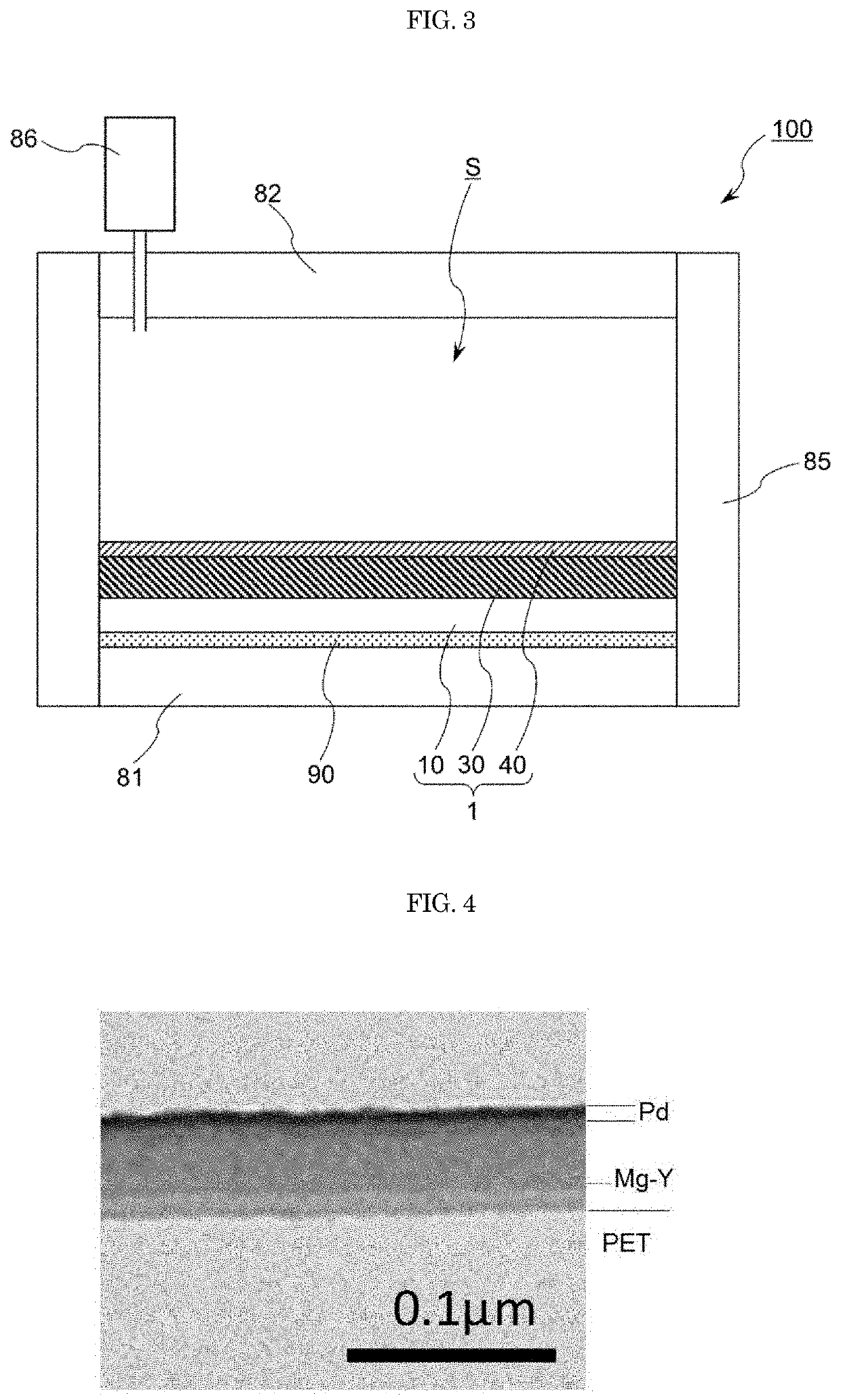
[0078]A roll of a 188 μm-thick polyethylene terephthalate (PET) film (manufactured by Mitsubishi Plastics, Inc.) was set in a roll-to-roll sputtering apparatus, and the inside of a sputtering apparatus was evacuated until the ultimate vacuum degree reached 5×10⁻³ Pa. The PET film substrate was conveyed in the sputtering apparatus without introducing a sputtering gas, and as a result, the internal pressure of the apparatus increased to 4×10⁻² Pa. This is because residual gas contained in the PET film was released into the sputtering apparatus.
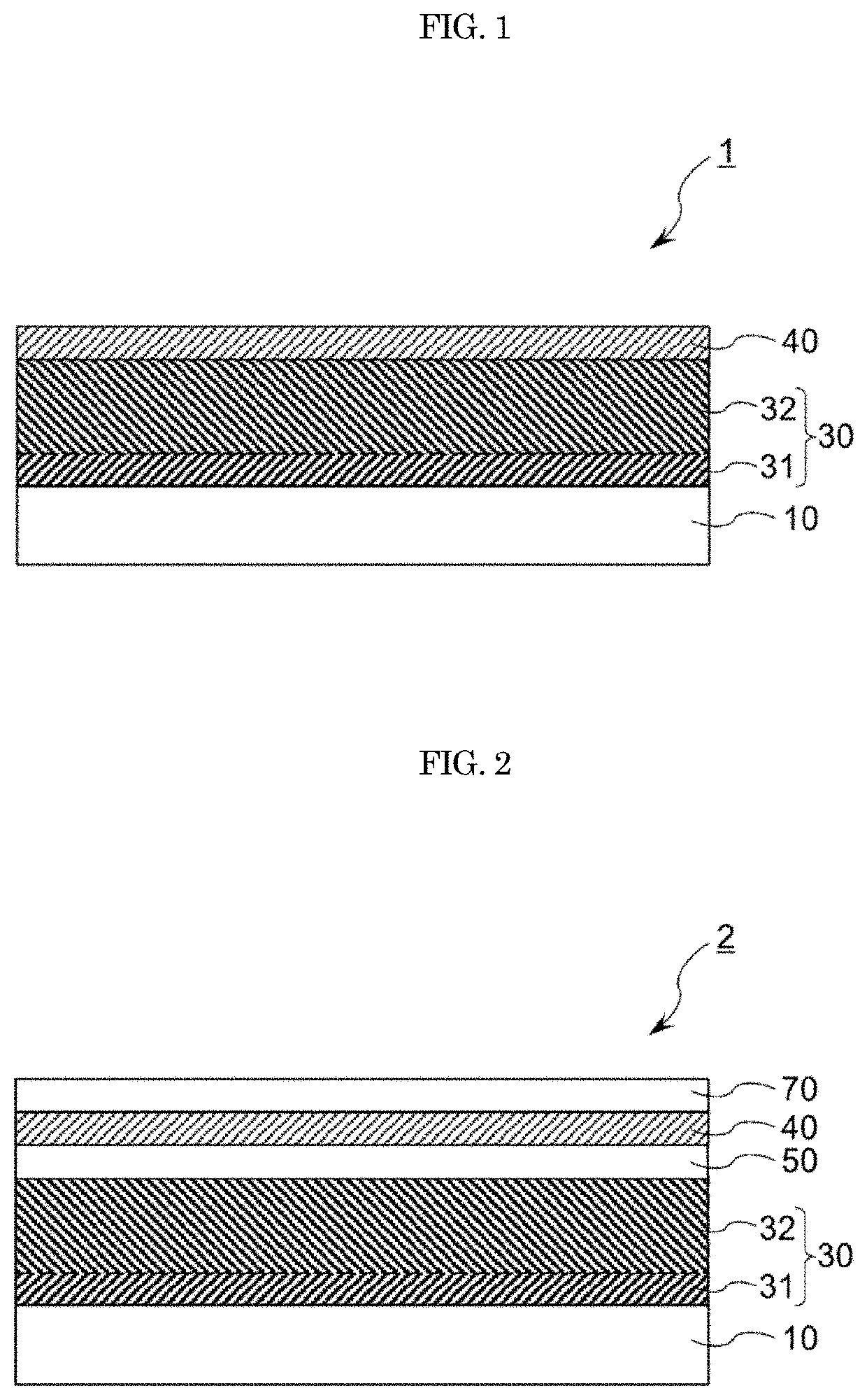
[0079]Thereafter, a sputtering gas was introduced into the sputtering apparatus, and a light modulation layer including an Mg—Y alloy and a catalyst layer including Pd were sequentially deposited while the film substrate was run on a deposition roll.
[0080]An Mg—Y split target (manufactured by RARE METALLIC Co., Ltd.) having an Mg metal plate and a Y metal plate at an erosion portion area ratio of 2:5 was used for deposition of the Mg—Y alloy lay...
example 2
[0082]Except that the ultimate vacuum degree before the start of sputtering deposition was 8×10⁻⁴ Pa, the same procedure as in Example 1 was carried out to prepare a light modulation film.
example 3
[0083]Except that the conditions for deposition of the light modulation layer were changed as described below, the same procedure as in Example 1 was carried out to prepare a light modulation film. In deposition of an Mg—Y alloy layer, first the Mg—Y alloy layer was formed in a thickness of 25 nm under 0.4 Pa vacuum environment in which 5% of oxygen in terms of a flow rate was introduced in argon as a sputtering gas. Subsequently, an Mg—Y alloy layer was formed in a thickness of 40 nm under an environment at 0.4 Pa with only argon introduced as a sputtering gas.
PUM
| Property | Measurement | Unit |
|---|---|---|
| thickness | aaaaa | aaaaa |
| thickness | aaaaa | aaaaa |
| thickness | aaaaa | aaaaa |
Abstract
Description
Claims
Application Information

