
Hinge structure and electronic device with the same

a technology of electronic devices and hinges, applied in the direction of casings/cabinets/drawers, casings with display/control units, instruments, etc., can solve the problems of affecting the safety of users, and affecting the safety of printed circuit boards in the display part. to prevent electric shocks or other dangerous situations

Active Publication Date: 2020-03-31
SAMSUNG ELECTRONICS CO LTD
View PDF12 Cites 2 Cited by
  • Summary
  • Abstract
  • Description
  • Claims
  • Application Information

AI Technical Summary

Benefits of technology

[0009]According to various embodiments of the disclosure, the case, which comes in direct contact with the user's skin, is configured to be insulated, thereby preventing electric shocks or other dangerous situations that the user may encounter when using the electronic device while charging the electronic device.
[0010]According to various embodiments of the disclosure, the case of the hinge structure may be insulated, and the hinge shafts may be interconnected, thereby providing a sufficient ground capacity for the printed circuit boards disposed in the main body part and / or the display part. The sufficient ground capacity allows for efficient hardware (H / W) capability (e.g., satisfactory ESD or wireless communication sensitivity) of the electronic device.

Problems solved by technology

However, if the paint coating peels off due to, e.g., scratches, current flow may be created through the cover.
Such current flow may cause an electric shock to the user, e.g., upon charging the electronic device.
As another example, when the main body part and the display part of the electronic device are produced to be electrically independent from each other, the printed circuit board embedded in the main body part may be vulnerable to electrostatic discharge (ESD) or electric shocks due to the shrunken ground.
The shrunken ground may also weaken the resistance of the printed circuit board in the display part to ESD or electric shocks.

Method used


Image

  • Hinge structure and electronic device with the same
  • Hinge structure and electronic device with the same
  • Hinge structure and electronic device with the same

Examples


Embodiment Construction

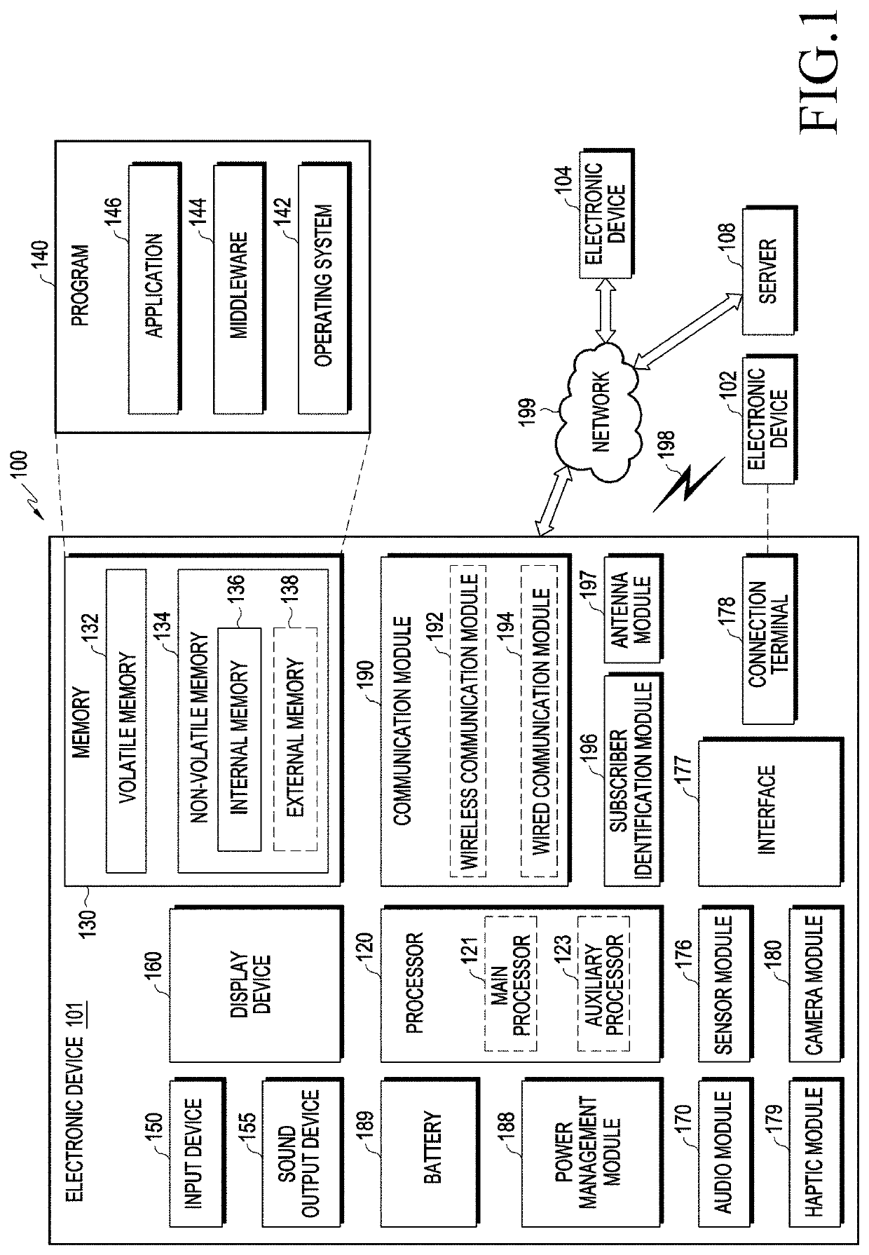
[0037]FIGS. 1 through 16, discussed below, and the various embodiments used to describe the principles of the present disclosure in this patent document are by way of illustration only and should not be construed in any way to limit the scope of the disclosure. Those skilled in the art will understand that the principles of the present disclosure may be implemented in any suitably arranged system or device.

[0038]The electronic device according to various embodiments may be one of various types of electronic devices. The electronic devices may include at least one of, e.g., a portable communication device (e.g., a smartphone), a computer device, a portable multimedia device, a portable medical device, a camera, a wearable device, or a home appliance. According to an embodiment of the disclosure, the electronic device is not limited to the above-listed embodiments.

[0039]It should be appreciated that various embodiments of the disclosure and the terms used therein are not intended to l...


PUM


Abstract

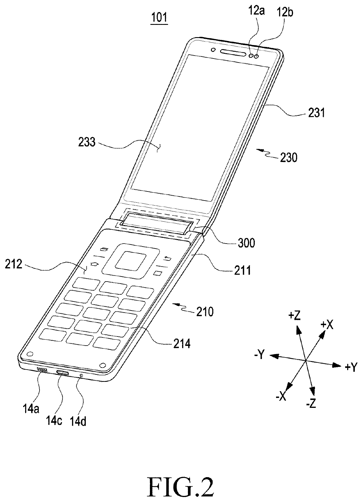
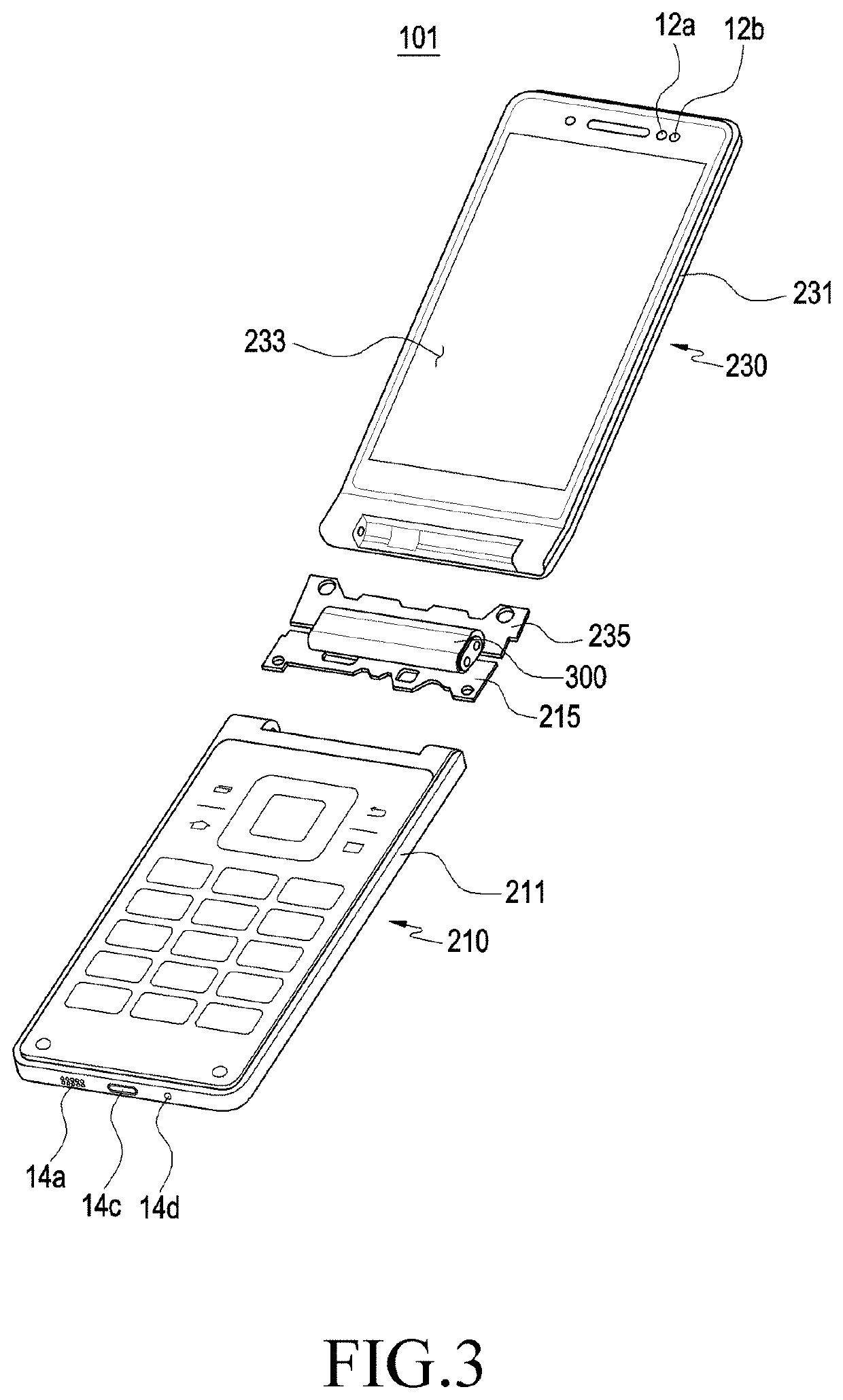
An electronic device may comprise a first housing structure including a first conductive part and a second housing structure including a second conductive part. The hinge structure may include a metallic bracket including a first conductive part and a second conductive part and a first cylindrical through hole and a second cylindrical through hole, a first cylindrical insulating bushing at least partially positioned inside the first through hole, a second cylindrical insulating bushing at least partially positioned inside the second through hole, a first conductive shaft contacting the first conductive part and extending through the first insulating bushing, a second conductive shaft contacting the second conductive part and extending through the second insulating bushing, and a conductive connector contacting the first conductive shaft and the second conductive shaft and configured to form an electrical path from the first conductive part to the second conductive part.

Description

CROSS-REFERENCE TO RELATED APPLICATIONS[0001]This application is based on and claims priority under 35 U.S.C. § 119 to Korean Patent Application No. 10-2017-0178675 filed on Dec. 22, 2017 in the Korean Intellectual Property Office, the disclosure of which is incorporated by reference herein in its entirety.BACKGROUND1. Field[0002]Various embodiments of the disclosure relate to hinge structures and electronic devices including the same.2. Description of Related Art[0003]The term “electronic device” may mean a device performing a particular function according to its equipped program, such as a home appliance, an electronic scheduler, a portable multimedia player, a mobile communication terminal, a tablet PC, a video / sound device, a desktop PC or laptop computer, a navigation device for an automobile, etc. For example, electronic devices may output stored information as voices or images. As electronic devices are highly integrated, and high-speed, high-volume wireless communication bec...

Claims


Application Information

Patent Timeline
Patent Type & Authority Patents(United States)
IPC IPC(8): E05D11/00H05K5/04H01R35/04H05K5/02H04M1/02H05K5/00H05K7/14E05D3/12
CPCE05D11/0081H05K5/0217H05K7/1427H05K5/0247H04M1/022H01R35/04H05K5/04E05D11/0054H05K5/0226H05K5/0017E05D3/122E05Y2900/606G06F1/1683G06F1/1681G06F1/1616
Inventor YOO, CHUNG KEUNHAN, YONG HWA
Owner SAMSUNG ELECTRONICS CO LTD
Learn More