Nonvolatile memory device, semiconductor device, and electronic apparatus

a nonvolatile memory, semiconductor technology, applied in information storage, static storage, instruments, etc., can solve the problems of increasing the load capacitance of the current mirror circuit, the inability to precisely set the determination reference, and the increase of the interconnect length, so as to improve the current supply capability of the reference cell and reduce the time it takes

Active Publication Date: 2020-04-07
SEIKO EPSON CORP
View PDF8 Cites 12 Cited by
  • Summary
  • Abstract
  • Description
  • Claims
  • Application Information

AI Technical Summary

Benefits of technology

[0009]An advantage of some aspects of the invention is to provide a nonvolatile memory device in which a determination reference is precisely set when verifying whether or not a memory cell is properly programmed to a programmed state in which the threshold voltage is high. Also, another advantage of some aspects of the invention is to improve the current supply capability of a reference cell used for generating a reference current so as to reduce the time it takes for the reference current to stabilize in a readout mode, in such a nonvolatile memory device. A further advantage of some aspects of the invention is to provide a semiconductor device, an electronic apparatus, and the like that use such a nonvolatile memory device.
[0014]Alternatively, the first reference cell may be set to the intermediate state between the erased state and the programmed state. With this, the current supply capability of the reference cell used for generating the reference current can be improved, and it is possible to reduce the time it takes for the reference current to stabilize in the readout mode. As a result, high-speed readout of data is made possible.
[0018]In the foregoing configurations, the second current mirror circuit may be configured such that a mirror ratio can be changed. Accordingly, the reference current can be changed with a simple configuration without increasing the number of reference cells or adjusting the drive potential of the reference cell, and the determination reference in the verify mode can be set.
[0021]Accordingly, in the readout mode, the amount of change in the reference current with respect to a change in the drive potential approximates the amount of change in the current flowing through the first reference cell, and as a result, the influence of a change in temperature or the power supply voltage can be reduced. Also, in the verify mode, the amount of change in the reference current with respect to the change in the drive potential is made relatively small, and as a result, the determination reference that is used when verifying whether or not the memory cell has been properly programmed can be precisely set.

Problems solved by technology

If such a reference current is used in the verify mode, the determination reference cannot be precisely set when verifying whether or not a memory cell is properly programmed.
Also, in the case where the number of bits of data that is read out at the same time in a readout mode is large, a current mirror circuit that generates a current corresponding to the current flowing through a reference cell is connected to a large number of sense amplifiers, and an interconnect length increases, and as a result, the load capacitance of the current mirror circuit increases, and it takes time for the reference current to stabilize.
Specifically, this problem becomes apparent with respect to the programmed state reference cell whose threshold voltage is high, because the current supply capability is low.

Method used


Image

  • Nonvolatile memory device, semiconductor device, and electronic apparatus
  • Nonvolatile memory device, semiconductor device, and electronic apparatus
  • Nonvolatile memory device, semiconductor device, and electronic apparatus

Examples


Embodiment Construction

[0031]Hereinafter, embodiments of the invention will be described in detail with reference to the drawings. The same constituent elements are given the same reference numerals, and a redundant description is omitted.

[0032]Although the invention can be applied to various types of electrically rewritable nonvolatile memory devices such as a flash memory and an EEPROM, in the following, an embodiment in which the invention is applied to a flash memory will be described as an example.

[0033]Overall Configuration of Nonvolatile Memory Device

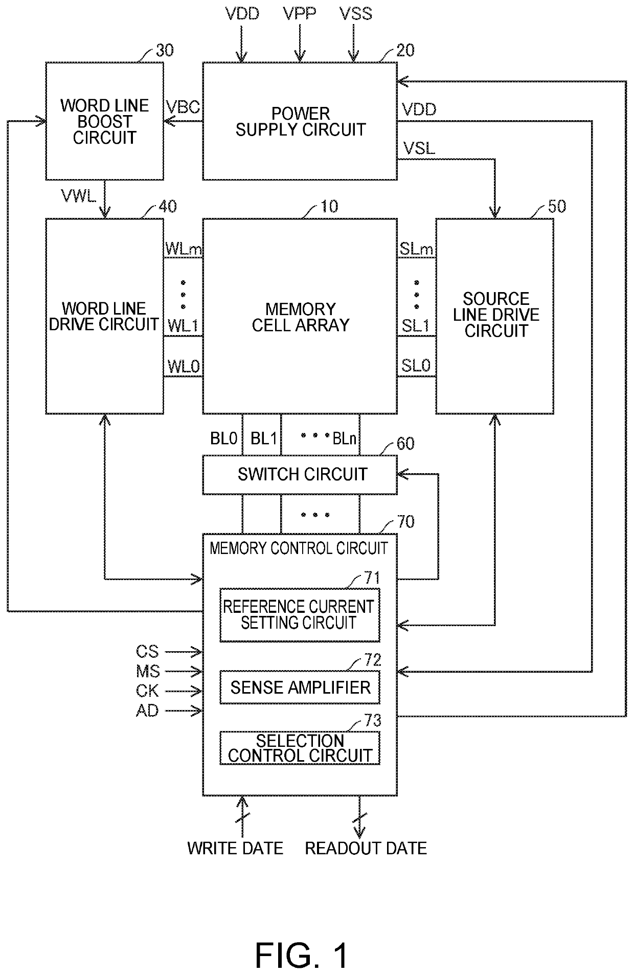
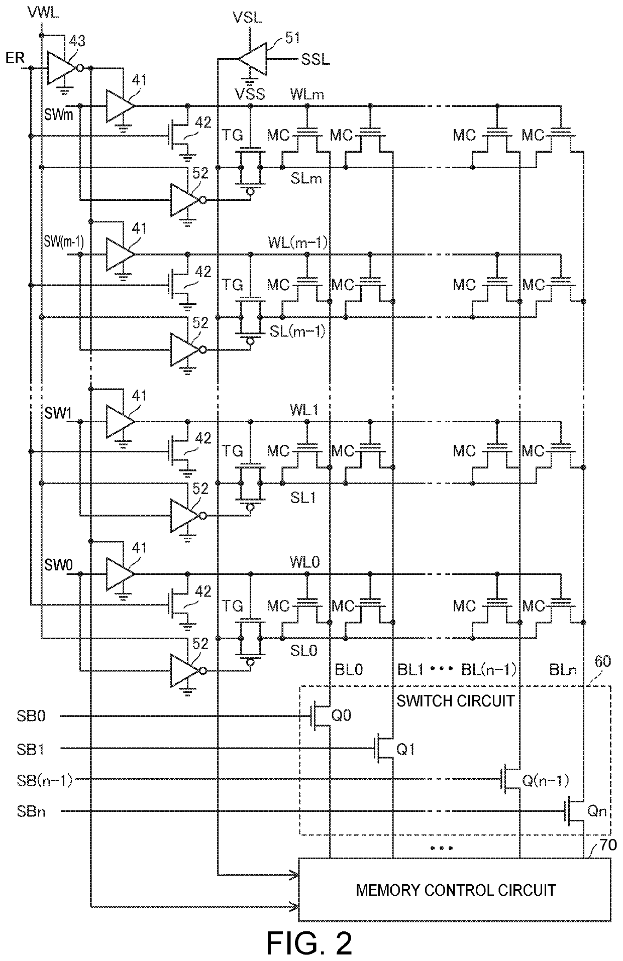
[0034]FIG. 1 is a block diagram illustrating an exemplary configuration of a nonvolatile memory device according to one embodiment of the invention. As shown in FIG. 1, the nonvolatile memory device includes a memory cell array 10, a power supply circuit 20, a word line boost circuit 30, a word line drive circuit 40, a source line drive circuit 50, a switch circuit 60, and a memory control circuit 70.

[0035]In the memory cell array 10, a plurality of me...


PUM


Abstract

A nonvolatile memory device includes: a first reference cell; a second reference cell; a circuit that generates a first mirror current proportional to a current flowing through the first reference cell; a circuit that generates a second mirror current proportional to a current flowing through the second reference cell; a sense amplifier that reads out data by comparing a current flowing through a memory cell with a reference current; and a selection circuit that sets a selection state of the first reference cell and the second reference cell such that, in a readout mode, the reference current is generated based on at least the first mirror current, and in a verify mode, the reference current is generated based on the second mirror current.

Description

CROSS REFERENCE[0001]This application claims priority to Japanese Patent Application No. 2017-097935, filed on May 17, 2017, the entire disclosure of which is expressly incorporated herein by reference.BACKGROUND1. Technical Field[0002]The present invention relates to electrically rewritable nonvolatile memory devices such as a flash memory and an EEPROM (Electrically Erasable Programmable Read-Only Memory). Furthermore, the invention relates to semiconductor devices, electronic apparatuses, and the like that use such nonvolatile memory devices.2. Related Art[0003]In recent years, electrically rewritable nonvolatile memory devices such as a flash memory and an EEPROM have come into wide used. In such nonvolatile memory devices, in order to determine whether a memory cell is in an erased state or in a programmed state, a reference current is generated based on currents that flow through a plurality of reference cells, and the current flowing through the memory cell is compared with t...

Claims


Application Information

Patent Timeline
Patent Type & Authority Patents(United States)
IPC IPC(8): G11C16/28G11C16/30G11C16/08G11C16/34G11C16/04
CPCG11C16/28G11C16/08G11C16/3459G11C16/30G11C16/0425G11C2207/063G11C16/0408G11C16/3404
Inventor MIYAZAKI, TAKESHI
Owner SEIKO EPSON CORP
Why Eureka
Try Eureka