Packaging material for power storage device and power storage device using the packaging material

a technology for power storage devices and packaging materials, which is applied in the manufacture of final products, secondary cells, synthetic resin layered products, etc., can solve the problems of pinholes and breakage, high degree of stretching, etc., and achieve the effect of preventing the decrease of the protection effect of the substrate layer, reducing the number of holes, and ensuring the formability

Active Publication Date: 2020-04-21
TOPPAN PRINTING CO LTD
View PDF19 Cites 0 Cited by
  • Summary
  • Abstract
  • Description
  • Claims
  • Application Information

AI Technical Summary

Benefits of technology

[0018]The present invention can provide a packaging material for a power storage device having a sufficient formability to better prevent decrease in protection effect of the substrate layer. Further, the present invention can provide a power storage device using the packaging material. With the power storage device using the packaging material for a power storage device according to the present invention, more contents can be efficiently accommodated to increase the energy density.

Problems solved by technology

However, as the recess depth increases, pinholes and breakage may often occur during a molding process by a mold at an edge or corner of the recess, which is a portion having a high degree of stretching.

Method used


Image

  • Packaging material for power storage device and power storage device using the packaging material
  • Packaging material for power storage device and power storage device using the packaging material
  • Packaging material for power storage device and power storage device using the packaging material

Examples


examples

[0104]The details of the present invention will be described below by way of Examples, but the present invention is not limited by the following description.

[0105][Materials for Use]

[0106]Materials used for the present Examples are shown below.

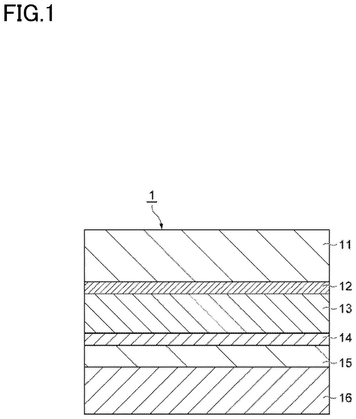
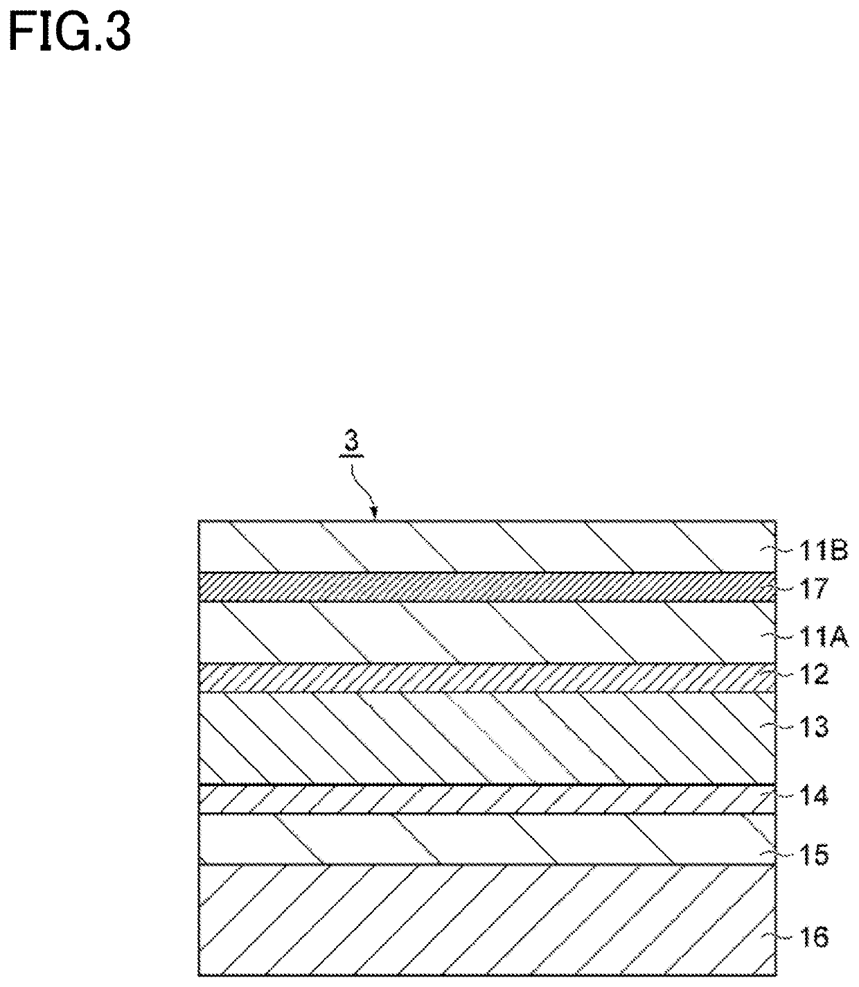
[0107](Substrate Layer 11)

[0108]Substrate A-1: Polyester film (thickness 9 μm).

[0109]Substrate A-2: Polyester film (thickness 12 μm).

[0110]Substrate A-3: Polyester film (thickness 15 μm).

[0111]Substrate A-4: Polyester film (thickness 25 μm).

[0112]Substrate A-5: Polyamide film (thickness 12 μm).

[0113]Substrate A-6: Polyamide film (thickness 15 μm).

[0114]Substrate A-7: Polyamide film (thickness 25 μm).

[0115]Substrate A-8: Polyester film (thickness 12 μm). A corona treatment is applied on the surface facing the adhesive layer.

[0116]Substrate A-9: Polyester film (thickness 12 μm). A frame treatment is applied on the surface facing the adhesive layer.

[0117]Substrate A-10: Polyester film (thickness 12 μm). A primer treatment is applied on the surfac...


PUM

PropertyMeasurementUnit
roughness Rzjisaaaaaaaaaa
peel strengthaaaaaaaaaa
thicknessaaaaaaaaaa

Abstract

The present invention relates to a packaging material for a power storage device including at least a substrate layer, an adhesive layer, a metal foil layer, an anti-corrosion treatment layer, an adhesive resin layer and a thermal bonding resin layer laminated in this order, wherein a thickness of the adhesive layer is in a range of 0.3 to 3 μm, a 10-point average roughness Rzjis (in accordance with JIS B0601) of a surface of the metal foil layer which faces the substrate layer is in a range of 0.3 to 3 μm, and the thickness of the adhesive layer is not less than the 10-point average roughness Rzjis and not more than 3 μm, and a peel strength between the substrate layer and the metal foil layer (in accordance with JIS K6854-3) is in a range of 5 to 12 N / 15 mm.

Description

CROSS-REFERENCE TO RELATED PATENT APPLICATIONS[0001]This application is a continuation application filed under 35 U.S.C. § 111(a) claiming the benefit under 35 U.S.C. §§ 120 and 365(c) of International Application No. PCT / JP2016 / 063427, filed on Apr. 28, 2016, which is based upon and claims the benefit of priority of Japanese Patent Application No. 2015-098831, filed on May 14, 2015, the entireties of which are hereby incorporated by reference.TECHNICAL FIELD[0002]The present invention relates to a packaging material for a power storage device and to a power storage device using the packaging material.BACKGROUND[0003]In recent years, ultra-thin and compact power storage devices have been actively developed for use in personal computers, mobile terminal devices such as cell phones, video cameras, satellites and vehicles. As a packaging material for such power storage devices, laminate packaging materials formed of a multi-layered film (for example, a configuration made up of a substr...

Claims


Application Information

Patent Timeline
Patent Type & Authority Patents(United States)
IPC IPC(8): H01M2/02B32B27/34B32B3/30B32B15/09B32B27/36B32B25/16B32B1/00B32B27/08B32B27/32H01G4/005B32B27/16B32B15/088B32B7/12H01M2/30H01G11/78B32B15/08B32B25/08H01G4/224H01G4/228H01M2/10H01M50/119H01M50/121H01M50/128H01M50/131H01M50/133H01M50/145H01M50/562
CPCB32B27/08H01M2/0287B32B7/12H01M2/30B32B27/36B32B1/00H01G11/78B32B15/08H01M2/1094B32B27/16B32B3/30H01G4/005B32B15/09B32B27/32B32B25/08H01M2/02H01M2/0285H01M2/028H01G4/228B32B25/16B32B15/088B32B27/34H01G4/224H01M2220/20B32B2307/50B32B2255/28B32B2274/00B32B2255/06B32B2457/00H01M2220/30B32B2255/26B32B2255/20B32B2553/00B32B2307/738B32B2307/538B32B2255/10B32B2307/752Y02E60/13H01M10/04H01M50/129H01M50/145H01M50/121Y02E60/10Y02P70/50H01M50/562H01M50/133H01M50/128H01M50/131H01M50/119C09J175/04B32B2307/714B32B2457/16H01M50/124H01M50/116H01M50/543H01M50/24
Inventor MUROI, YUKI
Owner TOPPAN PRINTING CO LTD
Why Eureka
Try Eureka