Single electron transistor triggered by photovoltaic diode

a photovoltaic diode and electron transistor technology, applied in the direction of optical radiation measurement, instruments, x/gamma/cosmic radiation measurement, etc., can solve the problems of silicon spads with significant wavelength limitations, silicon spads, and inability to detect the longer wavelengths within this rang

Active Publication Date: 2020-04-28
CHARLES STARK DRAPER LABORATORY
View PDF6 Cites 2 Cited by
  • Summary
  • Abstract
  • Description
  • Claims
  • Application Information

AI Technical Summary

Problems solved by technology

The best SPAD devices, by far, are made of silicon, however, silicon SPADs have significant wavelength limitations.
Due to the band edge of silicon, silicon SPADs only function at wavelengths <1000 nm, and also often are not very efficient at detection of the longer wavelengths within this range (in the near infrared).
However, InGaAs / InP SPADs are dramatically inferior to Si SPADs, with much higher dark count rates (output current when no photo-input exists), they do not operate at room temperature, and they are susceptible to after-pulsing while still having relatively low efficiencies of around 10%-20%. in additional, InGaAs / InP devices are significantly more expensive to fabricate than silicon devices.
But photomultiplier tubes are bulky devices requiring very high voltages to operate.
And while SNSPD offer the best performance of any single photon detector, they also require cooling below 10° K. Attempts also have been made to directly fabricate SPADs using germanium, but those devices have extremely high dark count rates, making them unsuitable for most applications.

Method used


Image

  • Single electron transistor triggered by photovoltaic diode
  • Single electron transistor triggered by photovoltaic diode

Examples


Embodiment Construction

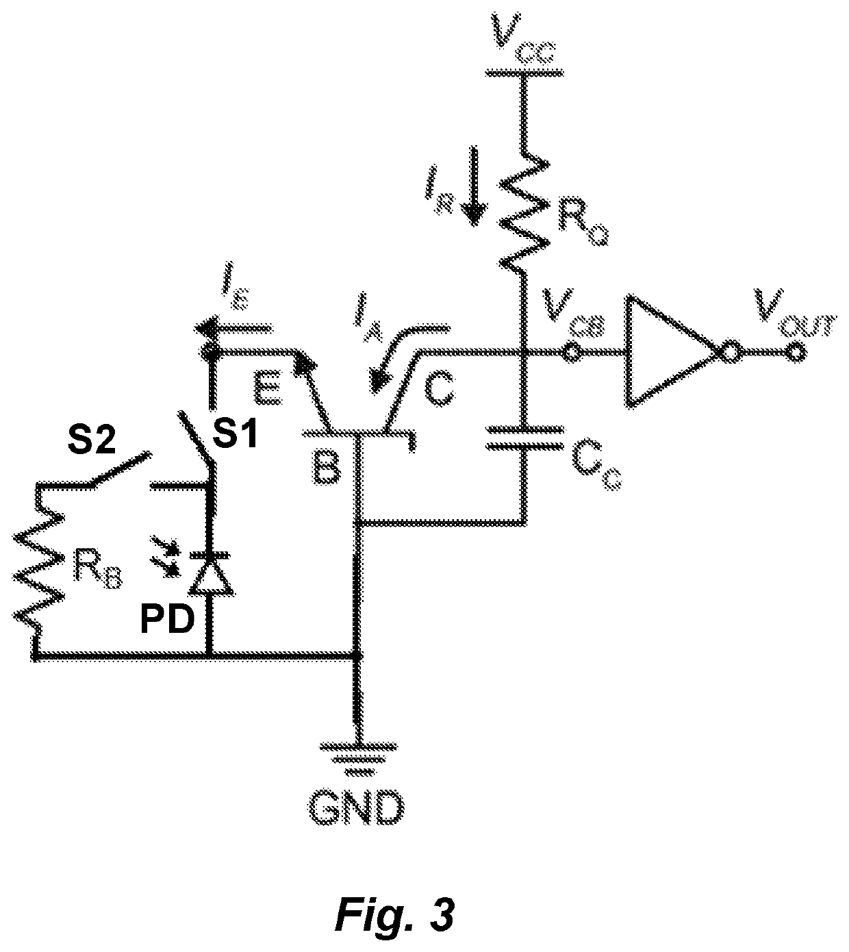
[0013]Various embodiments of the present invention are directed to a single photon detector that includes a germanium photodiode in combination with a single electron bipolar avalanche transistor (SEBAT). The resulting single photon detection circuit has excellent sensitivity, can operate at room temperature, has low dark counts, is silicon / CMOS process compatible, and is sensitive to wavelengths from about 700-1550 nm (wavelengths from 1400-1550 nm are of particular interest in LiDAR applications for eye-safety reasons).

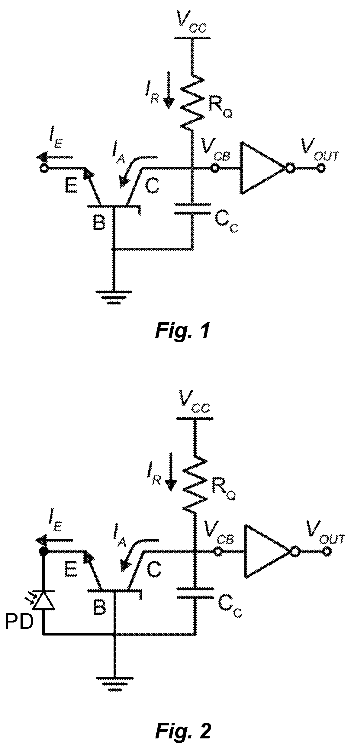
[0014]FIG. 1 shows an example of a single electron bipolar avalanche transistor (SEBAT) circuit as described in M. Lany, G. Boero and R. Popovic, “Electron counting at room temperature in an avalanche bipolar transistor,” Applied Physics Letters, vol. 92, p. 022111, 2008; and E. A. Webster, J. A. Richardson, L. A. Grant and R. K. Henderson, “A single electron bipolar avalanche transistor implemented in 90 nm CMOS,” Solid State Electronics, vol. 76, pp. 116-118, 2012...


PUM

PropertyMeasurementUnit
wavelengthsaaaaaaaaaa

Abstract

A single photon detection circuit is described that includes a germanium photodiode that is configured with zero voltage bias to avoid dark current output when no photon input is present and also is configured to respond to a single photon input by generating a photovoltaic output voltage. A single electron bipolar avalanche transistor (SEBAT) has a base emitter junction connected in parallel with the germanium photodiode and is configured so that the photovoltaic output voltage triggers an avalanche collector current output.

Description

[0001]This application claims priority from U.S. Provisional Patent Application 62 / 577,250, filed Oct. 26, 2017, which is incorporated herein by reference in its entirety.TECHNICAL FIELD[0002]The present invention relates to a single photon detection circuit suitable for detection of longer wavelength (infrared) input photons.BACKGROUND ART[0003]Single photon detection circuits are useful for a number of applications such as LiDAR, photoluminescence or fluorescence detection, and quantum information. One approach to detect single photons uses what is referred to as a single photon avalanche diode (SPAD), also sometimes called a Geiger-mode avalanche photodiode (GmAPD). In a SPAD, a photodiode is biased beyond breakdown and a single photon is all that is necessary to trigger the breakdown of the diode and create a large current that is easily detected.[0004]SPAD technology has the advantage of being semiconductor based so that it is compact, cheap, and reliable. The best SPAD devices...

Claims


Application Information

Patent Timeline
Patent Type & Authority Patents(United States)
IPC IPC(8): H01L31/02G01J1/02H01L31/107G01T1/24H01L31/111H01L31/028H01L29/73H04B10/70
CPCH01L31/107H01L31/02027H01L31/028H01L31/111G01T1/248G01J1/02H01L29/7313H04B10/70Y02E10/547
Inventor SPECTOR, STEVEN J.DAWSON, ROBIN MARK ADRIANMOEBIUS, MICHAEL G.LANE, BENJAMIN F.
Owner CHARLES STARK DRAPER LABORATORY
Why Eureka
Try Eureka