Check patentability & draft patents in minutes with Patsnap Eureka AI!

Over-voltage write operation of tunnel magnet-resistance (“TMR”) memory device and correcting failure bits therefrom by using on-the-fly bit failure detection and bit redundancy remapping techniques

a tunnel magnet-resistance memory and over-voltage write technology, applied in the field of random access memory (ram), can solve the problems of unreliability of memory, and characteristic failure rate, and achieve the effect of not incurring a large overhead to peripheral circuits

Active Publication Date: 2020-05-19
INTEGRATED SILICON SOLUTION CAYMAN INC
View PDF566 Cites 0 Cited by
  • Summary
  • Abstract
  • Description
  • Claims
  • Application Information

AI Technical Summary

Benefits of technology

The patent is about a system and method that can detect and correct bit defects in MRAM memory cells in real-time without needing to store any defective bits. The method uses redundancy bits added to each code to replace the defective bits, which reduces the amount of extra circuits needed. The system uses an algorithm to map the bad bits to their associated redundancy bits. The technical effects are that it allows for faster and more efficient replacement of bit defects in MRAM memory, improving the reliability and performance of these types of memory.

Problems solved by technology

The write failures are most generally random, and have a characteristic failure rate.
A high write error rate (WER) may make the memory unreliable.
The error rate can typically increase with age and increased use of the memory.
Bit-errors can result in system crashes, but even if a bit-error does not result in a system crash, it may cause severe problems because the error can linger in the system causing incorrect calculations and multiply itself into further data.
This is problematic especially in certain applications, e.g., financial, medical, automotive, etc. and is generally commercially unacceptable.
The corrupted data can also propagate to storage media and grow to an extent that is difficult to diagnose and recover.
Further, other conventional error correction schemes may require considerable overhead because the addresses / locations of all the bad bits in the memory chip need to be stored prior to performing the correction.
The Content Addressable Memories (CAMs) required to store such addresses and locations occupy significant surface area and are expensive because of the high overhead involved in saving the bit addresses / locations for all the failing bits.
Further, storing addresses of bad bits and then replacing them with good bits is also not an optimal scheme for STT-MRAM memories because the defect rate is typically high and too much memory would be required to store the addresses of all the bad bits.
Also, this error mitigation scheme does not work for defects that are discovered on-the-fly (e.g. replacing the bad bits with good bits may have only happened at the tester phase in manufacturing).
Further, typically, error schemes like ECC can detect and correct errors during a read operation, but it does not write the data back into the memory array.
This behavior causes the error to stay resident inside the memory array across multiple accesses and may contribute to a memory failure at a later time when additional errors occur.
For example, if the memory is used for longer periods of time, there is an increased probability of a second failure occurring in the same ‘word’ as a first failure.
The first failure may lie silently for years as the internal ECC logic repairs the error every time the word is read.
. . ) error hits the same word, the internal ECC circuitry is unable to repair the word and corrupted read data is provided to the system.
Additionally, ECC is not efficient for correcting high fixed defect rates.
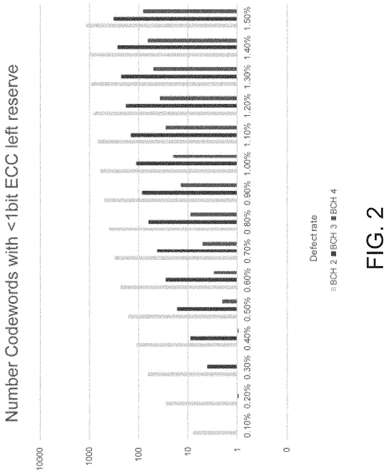
This is particularly problematic for memories comprising STT-MRAM that typically have higher failure rates as compared to other memories. FIG. 2 illustrates the number of codewords with less than 1 bit ECC left reserved as a function of the defect rate.
For memories with higher defect rates ECC and other error correction schemes become problematic.
Accordingly, in memory applications comprising STT-MRAM where defect rates are higher, using only conventional error mitigation schemes like ECC results in inefficiencies.

Method used


Image

  • Over-voltage write operation of tunnel magnet-resistance (“TMR”) memory device and correcting failure bits therefrom by using on-the-fly bit failure detection and bit redundancy remapping techniques
  • Over-voltage write operation of tunnel magnet-resistance (“TMR”) memory device and correcting failure bits therefrom by using on-the-fly bit failure detection and bit redundancy remapping techniques
  • Over-voltage write operation of tunnel magnet-resistance (“TMR”) memory device and correcting failure bits therefrom by using on-the-fly bit failure detection and bit redundancy remapping techniques

Examples


Embodiment Construction

[0038]Reference will now be made in detail to the various embodiments of the present disclosure, examples of which are illustrated in the accompanying drawings. While described in conjunction with these embodiments, it will be understood that they are not intended to limit the disclosure to these embodiments. On the contrary, the disclosure is intended to cover alternatives, modifications and equivalents, which may be included within the spirit and scope of the disclosure as defined by the appended claims. Furthermore, in the following detailed description of the present disclosure, numerous specific details are set forth in order to provide a thorough understanding of the present disclosure. However, it will be understood that the present disclosure may be practiced without these specific details. In other instances, well-known methods, procedures, components, and circuits have not been described in detail so as not to unnecessarily obscure aspects of the present disclosure.

[0039]S...


PUM


Abstract

A method for correcting bit defects in an STT-MRAM memory is disclosed. The method includes reading a codeword in the STT-MRAM memory, wherein the STT-MRAM memory includes a plurality of codewords, wherein each codeword includes a plurality of redundant bits. Further, the method includes mapping defective bits in the codeword to redundant bits of the plurality of redundant bits based on a mapping scheme, wherein the mapping scheme is operable to determine a manner in which the defective bits in the codeword are to be mapped to the redundant bits. Finally, the method includes replacing the defective bits in the codeword with corresponding mapped redundant bits.

Description

CROSS-REFERENCE TO RELATED APPLICATIONS[0001]The present application is a Continuation-in-Part of, claims the benefit of and priority to U.S. application Ser. No. 15 / 792,672, filed Oct. 24, 2017, entitled “ON-THE-FLY BIT FAILURE DETECTION AND BIT REDUNDANCY REMAPPING TECHNIQUES TO CORRECT FOR FIXED BIT DEFECTS” and hereby incorporated by reference in its entirety.FIELD[0002]The present patent document relates generally to random access memory (RAM). More particularly, the present patent document relates to failure detection and correction operations in magnetoresistive random-access-memory (“MRAM”). The methods and devices described herein are particularly useful in spin-transfer torque magnetic memory (STT-MRAM) devices.BACKGROUND[0003]Magnetoresistive random-access memory (“MRAM”) is a non-volatile memory technology that stores data through magnetic storage elements. These elements are two ferromagnetic plates or electrodes that can hold a magnetic field and are separated by a non...

Claims


Application Information

Patent Timeline
Patent Type & Authority Patents(United States)
IPC IPC(8): G06F11/00G11C29/42G11C29/52G06F11/10G11C11/16G11C29/04
CPCG11C29/42G06F11/1068G06F11/1048G11C29/52G11C11/1675G11C11/1673G11C11/1653G11C2029/0411
Inventor BERGER, NEALLOUIE, BENJAMINEL-BARAJI, MOURADCRUDELE, LESTER
Owner INTEGRATED SILICON SOLUTION CAYMAN INC
Features
  • R&D
  • Intellectual Property
  • Life Sciences
  • Materials
  • Tech Scout
  • Unparalleled Data Quality
  • Higher Quality Content
  • 60% Fewer Hallucinations
Learn More