

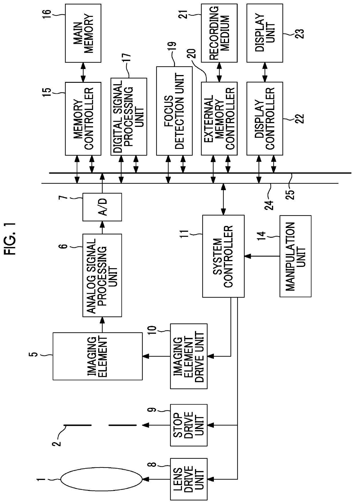
Imaging element and imaging device
a technology of imaging element and image, which is applied in the direction of instruments, television systems, color signal processing circuits, etc., can solve the problems of insufficient use of the output signal of the phase-difference detecting pixel as a pixel signal, and the quality of the captured image will deteriorate through correction, so as to improve the quality of the captured image
- Summary
- Abstract
- Description
- Claims
- Application Information
AI Technical Summary
Benefits of technology
Problems solved by technology
Method used
Image

Examples
first modification example
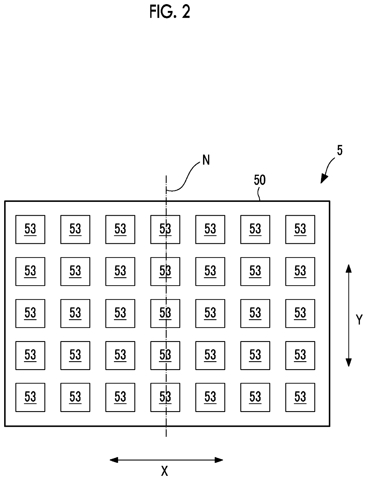
[0118]FIG. 8 is an enlarged schematic diagram showing a first modification example of the light receiving surface 50 shown in FIG. 2.
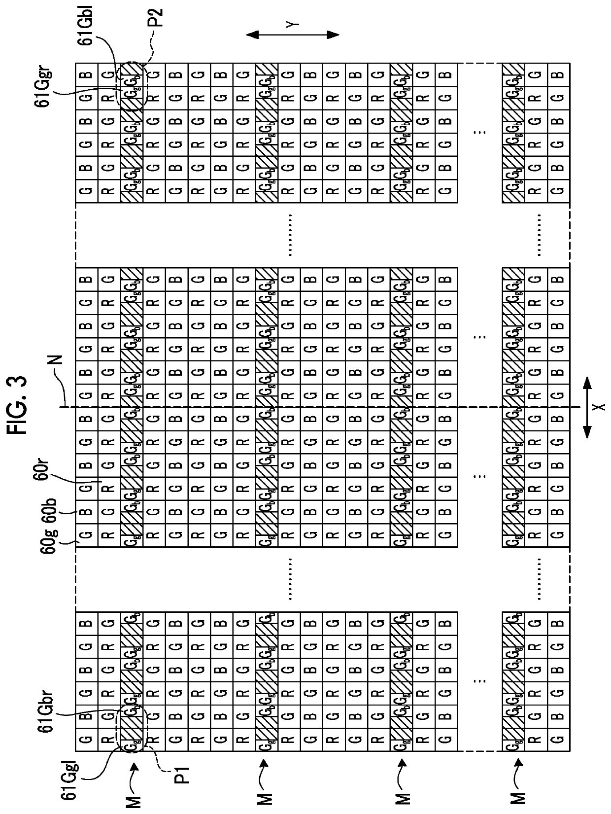
[0119]Phase-difference detecting pixel rows having two patterns such as first phase-difference detecting pixel rows M1 and second phase-difference detecting pixel rows M2 are formed in the imaging element 5 according to the first modification example shown in FIG. 8, instead of the phase-difference detecting pixel rows M. Other configurations are the same as those shown in FIG. 3.
[0120]In the first phase-difference detecting pixel row M1, a boundary between a portion in which the first pairs P1 are arranged and a portion in which the second pairs P2 are arranged is determined by a straight line N1 which is parallel to the straight line N and is present so as to be shifted from the straight line N in the right direction by two pixels.
[0121]In this example, a distance between the straight line N1 and the straight line N corresponds to two pixels, but thi...
second modification example
[0137]FIG. 9 is an enlarged schematic diagram showing a second modification example of the light receiving surface 50 shown in FIG. 2.
[0138]The imaging element 5 according to the second modification example shown in FIG. 9 is different from the imaging element 5 according to the first modification example in that the first phase-difference detecting pixel rows M1 and the second phase-difference detecting pixel rows M2 are alternately arranged with periodicity at an interval of N (in the example of FIG. 9, 2), N being a natural number of 2 or more, in the column direction Y. Other configurations are the same as those of the imaging element 5 according to the first modification example.
[0139]For example, in the configuration of the second modification example, at least of the straight line N1 or the straight line N2 is set in an area between each of the five phase-difference detecting areas 53 present in the center in the row direction X of FIG. 2 and the phase-difference detecting ar...
third modification example
[0151]It has been described in the first modification example and the second modification example that the first phase-difference detecting pixel rows M1 and the second phase-difference detecting pixel rows M2 are periodically arranged in the column direction Y.
[0152]In this modification example, the first phase-difference detecting pixel rows M1 and the second phase-difference detecting pixel rows M2 may be randomly arranged in the column direction Y. In such a configuration, it is possible to improve the quality of the captured image.
PUM
 Abstract
Description
Claims
Application Information