
Imaging element and imaging device

a technology of imaging element and image, which is applied in the direction of instruments, television systems, color signal processing circuits, etc., can solve the problems of insufficient use of the output signal of the phase-difference detecting pixel as a pixel signal, and the quality of the captured image will deteriorate through correction, so as to improve the quality of the captured image

Active Publication Date: 2019-03-28
FUJIFILM CORP
View PDF0 Cites 2 Cited by
  • Summary
  • Abstract
  • Description
  • Claims
  • Application Information

AI Technical Summary

Benefits of technology

The present invention aims to provide an imaging element and device that can improve the quality of captured images by using gain correction to correct the output signals of phase-difference detecting pixels. These pixels make a significant contribution to brightness signals and can improve image quality even at lower resolutions. Overall, the invention allows for improved image quality with minimal impact on the overall solution design.

Problems solved by technology

Thus, it is insufficient in using an output signal of the phase-difference detecting pixel as a pixel signal for generating captured image data.
Thus, in a case where a subject having a fine pattern is captured, there is a possibility that the quality of the captured image will deteriorate through the correction.

Method used


Image

  • Imaging element and imaging device
  • Imaging element and imaging device
  • Imaging element and imaging device

Examples


first modification example

[0118]FIG. 8 is an enlarged schematic diagram showing a first modification example of the light receiving surface 50 shown in FIG. 2.

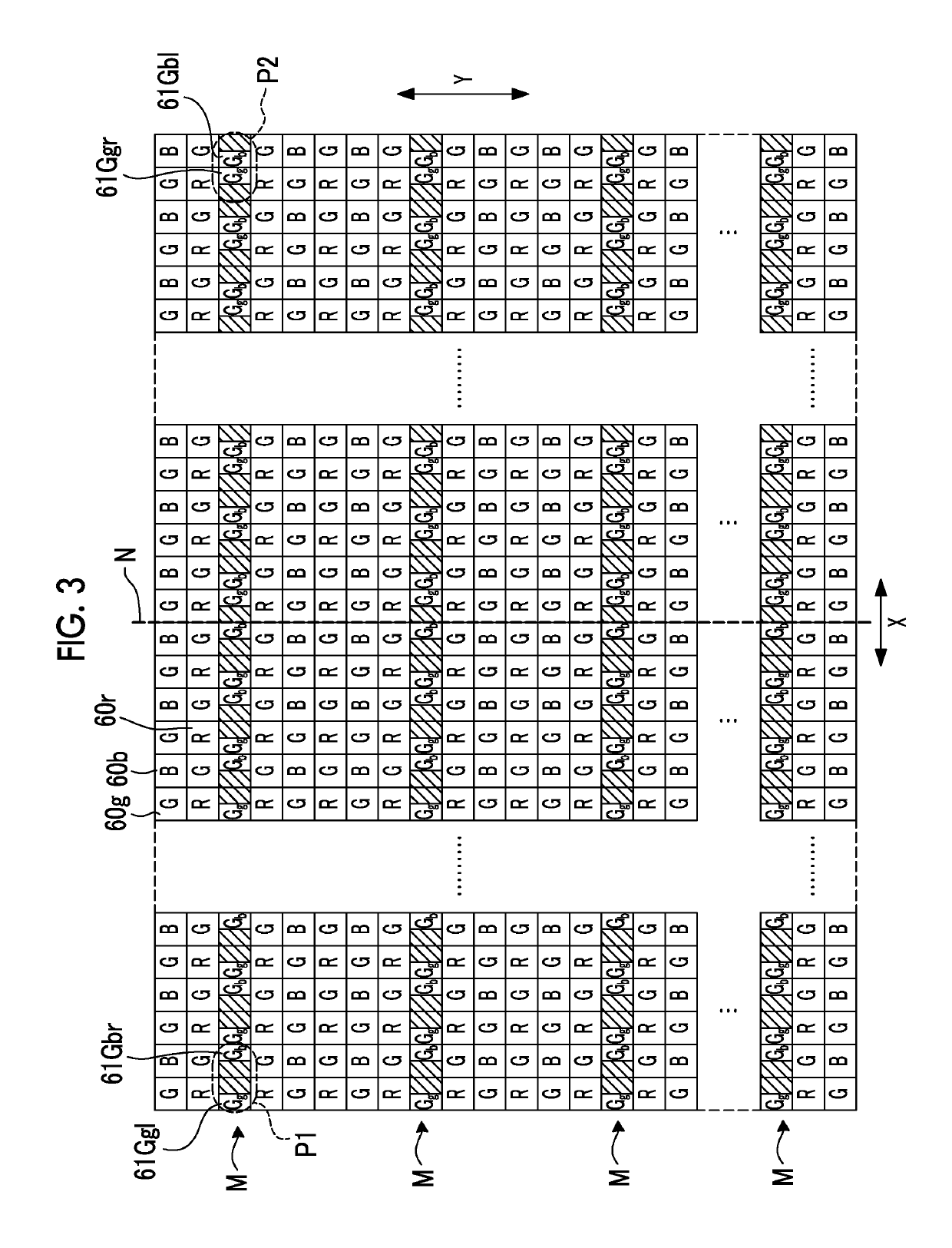
[0119]Phase-difference detecting pixel rows having two patterns such as first phase-difference detecting pixel rows M1 and second phase-difference detecting pixel rows M2 are formed in the imaging element 5 according to the first modification example shown in FIG. 8, instead of the phase-difference detecting pixel rows M. Other configurations are the same as those shown in FIG. 3.

[0120]In the first phase-difference detecting pixel row M1, a boundary between a portion in which the first pairs P1 are arranged and a portion in which the second pairs P2 are arranged is determined by a straight line N1 which is parallel to the straight line N and is present so as to be shifted from the straight line N in the right direction by two pixels.

[0121]In this example, a distance between the straight line N1 and the straight line N corresponds to two pixels, but thi...

second modification example

[0137]FIG. 9 is an enlarged schematic diagram showing a second modification example of the light receiving surface 50 shown in FIG. 2.

[0138]The imaging element 5 according to the second modification example shown in FIG. 9 is different from the imaging element 5 according to the first modification example in that the first phase-difference detecting pixel rows M1 and the second phase-difference detecting pixel rows M2 are alternately arranged with periodicity at an interval of N (in the example of FIG. 9, 2), N being a natural number of 2 or more, in the column direction Y. Other configurations are the same as those of the imaging element 5 according to the first modification example.

[0139]For example, in the configuration of the second modification example, at least of the straight line N1 or the straight line N2 is set in an area between each of the five phase-difference detecting areas 53 present in the center in the row direction X of FIG. 2 and the phase-difference detecting ar...

third modification example

[0151]It has been described in the first modification example and the second modification example that the first phase-difference detecting pixel rows M1 and the second phase-difference detecting pixel rows M2 are periodically arranged in the column direction Y.

[0152]In this modification example, the first phase-difference detecting pixel rows M1 and the second phase-difference detecting pixel rows M2 may be randomly arranged in the column direction Y. In such a configuration, it is possible to improve the quality of the captured image.


PUM


Abstract

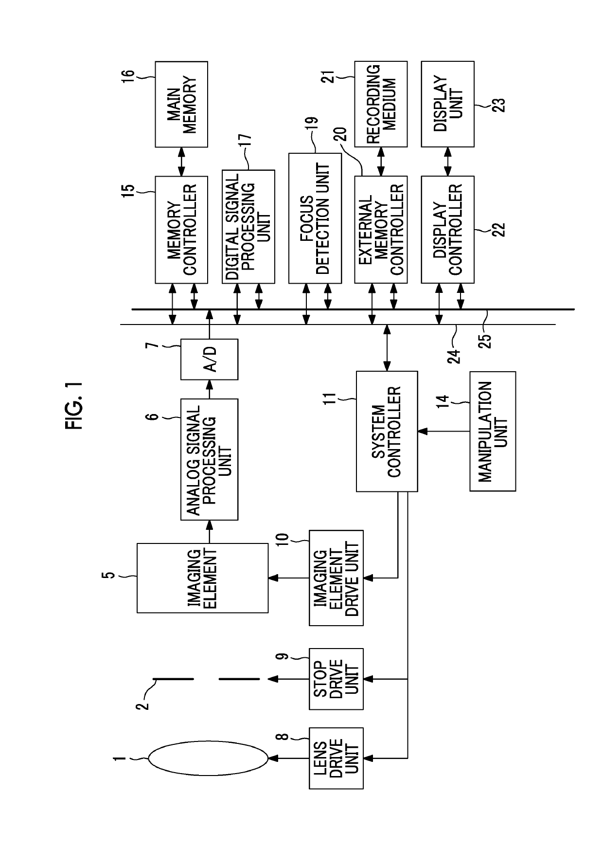
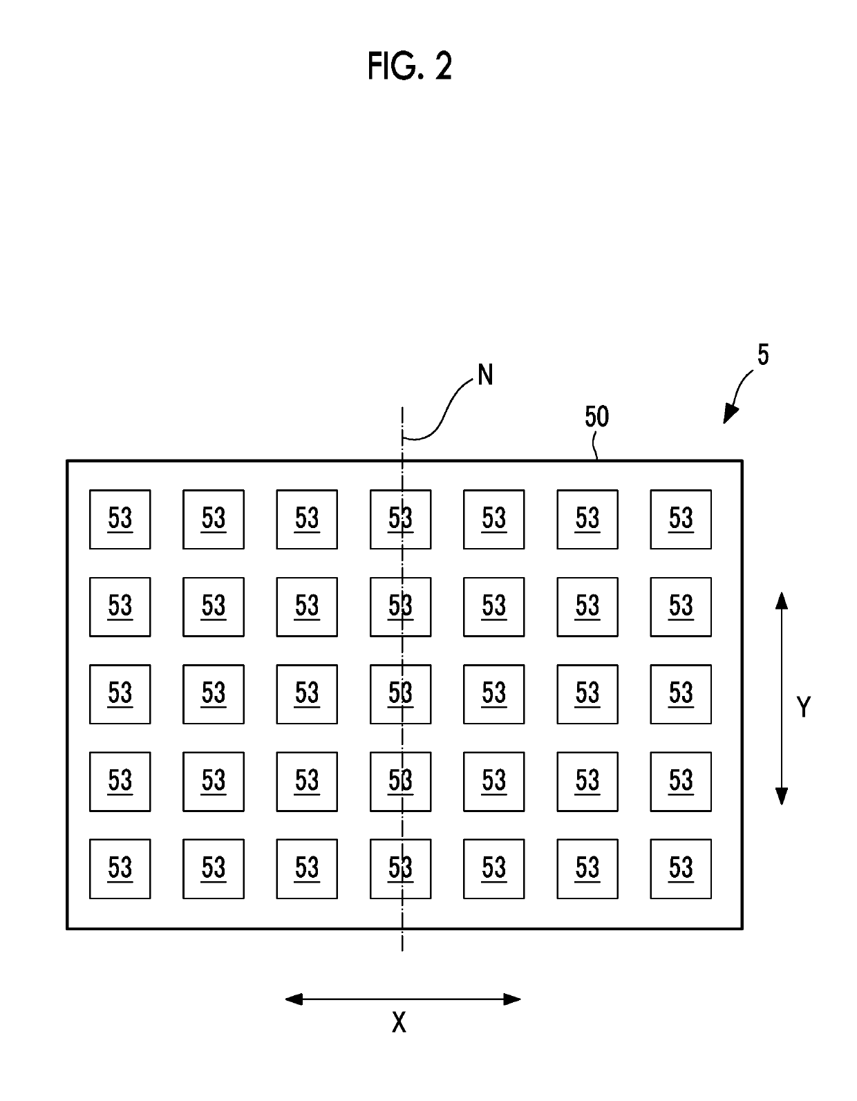
An imaging element has plural pixels which photoelectrically convert light rays having different colors, and has a light receiving surface on which the plural pixels are arranged in two dimensions according to a regular pattern, the plural pixels include first pixels that output signals each having a first color component which most contribute to obtainment of brightness signals, and second pixels that output signals having color components other than the first color component, the first pixels and the second pixels are as defined herein, and a pair row is formed on the light receiving surface as defined herein.

Description

CROSS REFERENCE TO RELATED APPLICATION[0001]This is a continuation of International Application No. PCT / JP2017 / 016820 filed on Apr. 27, 2017, and claims priority from Japanese Patent Application No. 2016-110393 filed on Jun. 1, 2016, the entire disclosures of which are incorporated herein by reference.BACKGROUND OF THE INVENTION1. Field of the Invention[0002]The present invention relates to an imaging element and an imaging device.2. Description of the Related Art[0003]With an increase in resolution of imaging elements, such as a charge coupled device (CCD) image sensor and a complementary metal oxide semiconductor (CMOS) image sensor, there is a rapid increase in demand for information devices having an imaging function, such as a digital still camera, a digital video camera, and a mobile phone such as a smartphone. The information devices having an imaging function described above are referred to as imaging devices.[0004]In these imaging devices, a phase difference auto focus (AF)...

Claims


Application Information

Patent Timeline
Patent Type & Authority Applications(United States)
IPC IPC(8): H04N5/369H04N23/12
CPCH04N5/36961G02B7/34G03B13/36H04N23/672H04N25/704H04N25/70H04N23/843H04N25/134H04N23/84H04N9/64
Inventor KOBAYASHI
Owner FUJIFILM CORP
Learn More