Method of advanced contact hole pattering

a contact hole and advanced technology, applied in the field of microfabrication, can solve the problems of reducing throughput, reducing the processing time of photolithography exposure tools, and reducing the yield of final products, so as to improve the definition of patterns, reduce lcdu, and prolong processing time

Active Publication Date: 2020-08-04
TOKYO ELECTRON LTD
View PDF0 Cites 1 Cited by
  • Summary
  • Abstract
  • Description
  • Claims
  • Application Information

AI Technical Summary

Benefits of technology

[0005]Local critical dimension uniformity (LCDU) is defined in a lithography step and is related inversely by the square root of the number of photons. Thus, as the number of photons increases, the pattern definition improves and a theoretically lower LCDU is attainable. Using more photons, however, means significantly longer processing time on a photolithography exposure tool (scanner, stepper) which means reduced throughput. With time spent on a photolithography tool being the largest portion of microfabrication cost, much effort is spent to reduce time on such tools.
[0006]Techniques herein include a method of forming contact holes. Techniques herein use a reversal method to create contact hole patterns with improved LCDU and CER (Contact Edge Roughness) as compared to traditional direct print photolithography methods. Instead of printing a hole, a pillar is printed as an initial structure. Printing (patterned actinic radiation exposure) pillars instead of holes enables using a same pitch as designed for a final hole, but with a larger scanner dose-bias. This allows printing the initial feature using more photons, which reduces stochastic effects contributed by a given photolithographic light source. With reversal techniques herein, the impact of LCDU and CER in the final printed hole can be reduced because the initial structure can use a larger maximum number photons to define the pattern.
[0007]One embodiment includes a method of forming a patterned mask having contact openings. This method includes forming a relief pattern of pillars (pillars structures) on a working surface of a substrate. The pillars protrude from the working surface of the substrate. A reshaping process is executed that modifies a shape of the pillars by rounding a profile of the pillars, or shrinking the pillars, and / or reducing roughness of the pillars. A first conformal film is deposited on the substrate, the first conformal film can include a hardmask material or metal-containing material. A planarization process is executed that removes pillars down to the working surface of the substrate leaving the first conformal film on the working surface of the substrate. This conformal film can then be used as an etch mask for pattern transfer.

Problems solved by technology

This result is in part affected by a number or amount of photons that can pass through a mask—especially as a target pitch used is at the resolution limits of conventional photolithography systems.
This is undesirable because a single closed hole results in a 100% loss in yield in the final product die.
Using more photons, however, means significantly longer processing time on a photolithography exposure tool (scanner, stepper) which means reduced throughput.
With time spent on a photolithography tool being the largest portion of microfabrication cost, much effort is spent to reduce time on such tools.

Method used


Image

  • Method of advanced contact hole pattering
  • Method of advanced contact hole pattering
  • Method of advanced contact hole pattering

Examples


Embodiment Construction

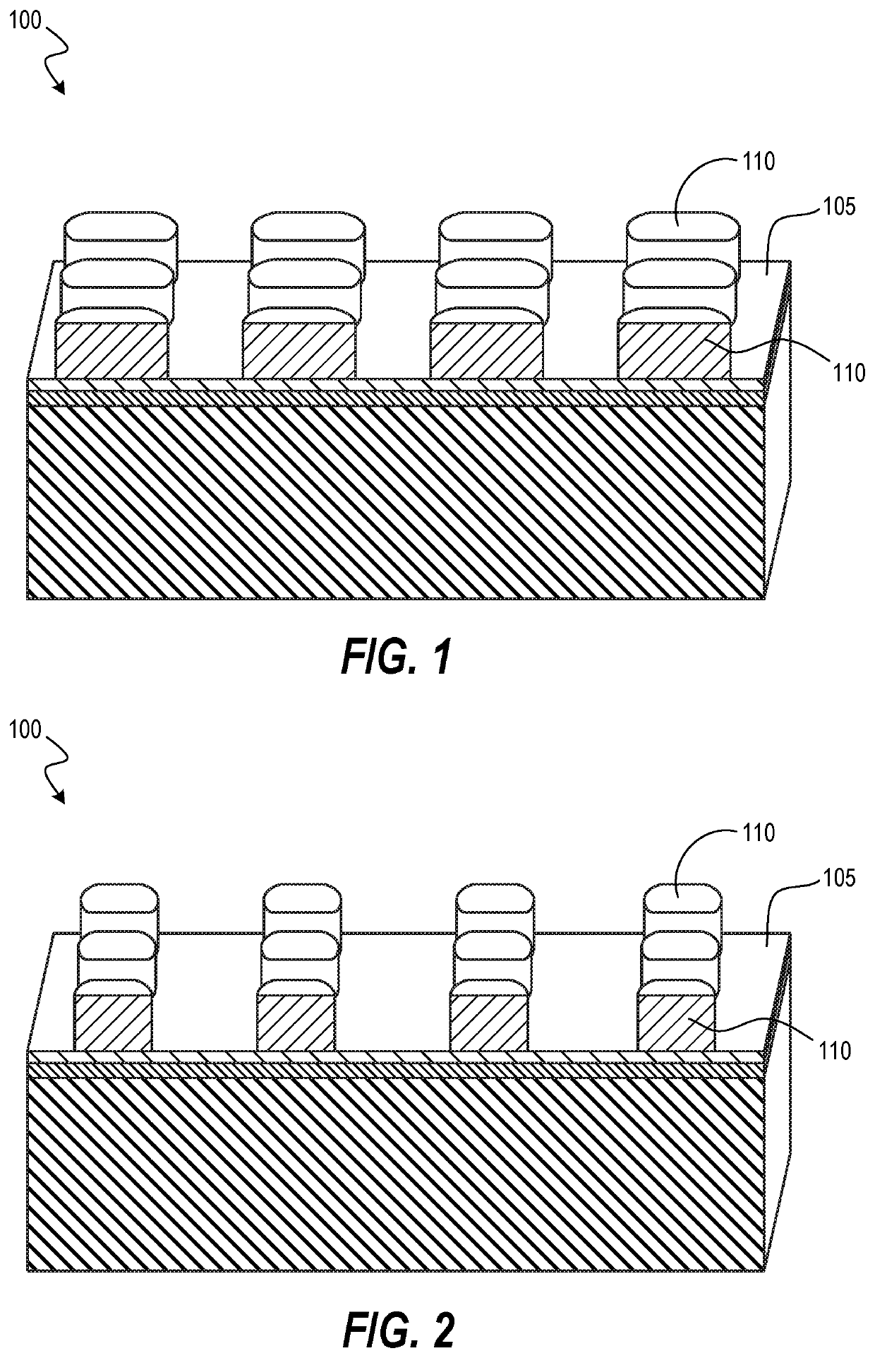
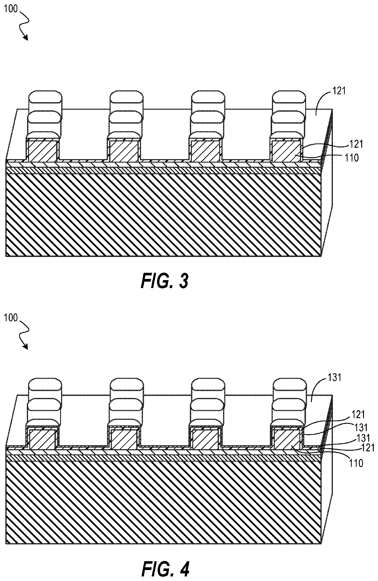
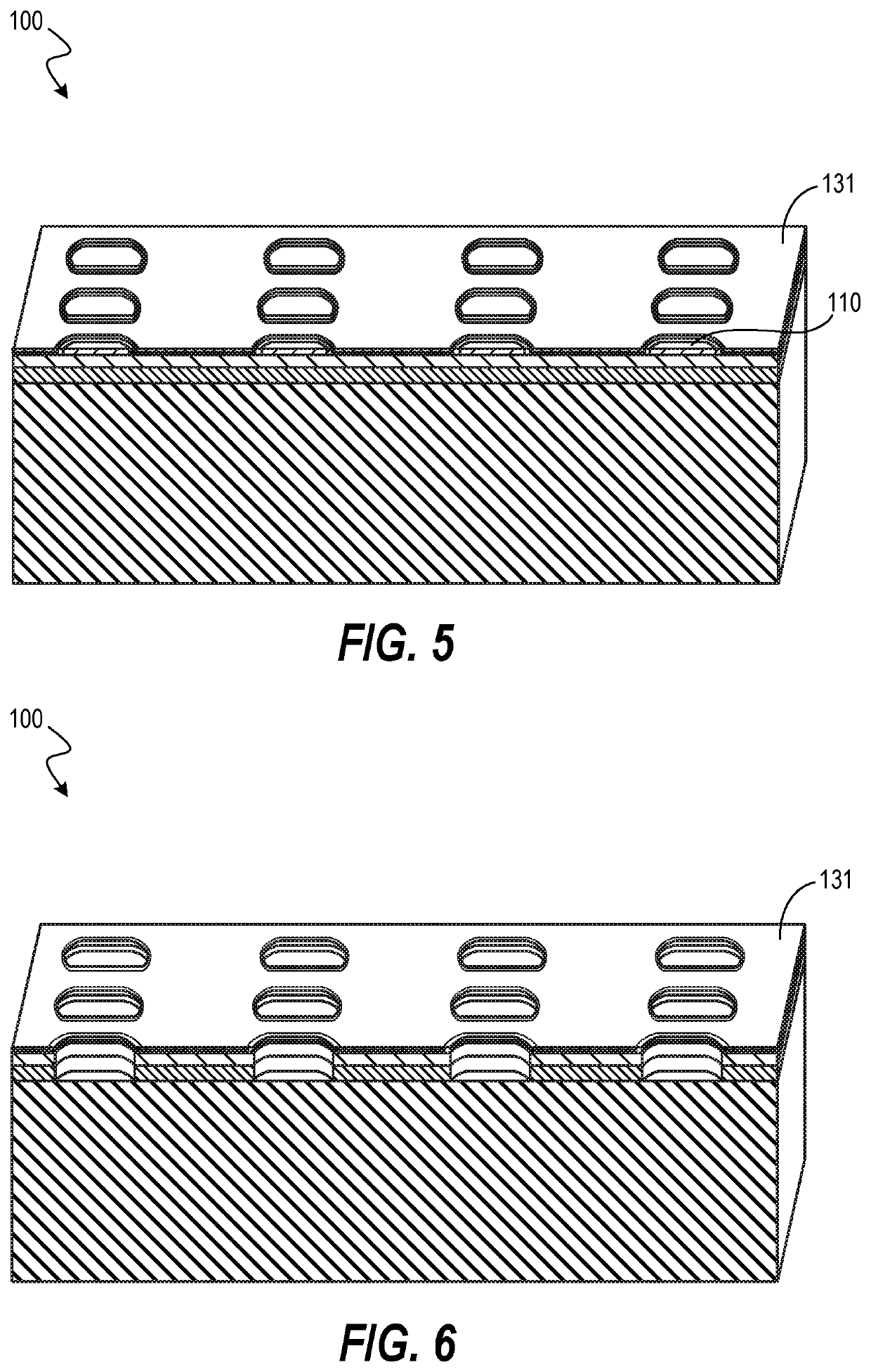
[0025]Techniques herein include methods for uniform and accurate patterning for microfabrication of various structures and features including contact holes. One technique includes printing and forming an initial size / shape pillar in a relief pattern, and then modifying that pillar and reversing the pattern as a method for generating an etch mask. For example, a larger dimension pillar structure, as compared to a target hole dimension desired, is printed in a layer of photoresist on a substrate, which can then be transferred to an underlying material (such as a carbon hardmask) to facilitate additional processing. Alternatively, the pillar formed of photoresist can be used / modified prior to transfer to an underlying layer. This printed pillar, having an initial size and shape, can then be modified. For example, the pillar can be resized and / or reshaped to a smaller dimension pillar or bump-shaped structure and / or a smoother pillar surface. Additional smoothing can be realized using a...


PUM

PropertyMeasurementUnit
thicknessaaaaaaaaaa
angleaaaaaaaaaa
thicknessesaaaaaaaaaa

Abstract

Techniques herein include a method of forming etch masks to form contact holes and other features. Techniques herein use a reversal method to create contact hole patterns with improved critical dimension uniformity and contact edge roughness as compared to traditional direct print photolithography methods. A pillar is printed as an initial structure. The initial structure is reshaped to change smoothness, uniformity, and / or dimensions. A conformal film is deposited on the pillar. The conformal film can include a metal-containing material. A planarization process is executed that removes pillars down to the working surface of the substrate leaving the conformal film on the working surface of the substrate. This conformal film can then be used as an etch mask for additional pattern transfer.

Description

CROSS REFERENCE TO RELATED APPLICATIONS[0001]The present application claims the benefit of U.S. Provisional Patent Application No. 62 / 614,244, filed on Jan. 5, 2018, entitled “Method of Advanced Contact Hole Patterning,” which is incorporated herein by reference in its entirety.BACKGROUND OF THE INVENTION[0002]Techniques disclosed herein relate to microfabrication, and relate in particular to photolithography.[0003]In material processing methodologies (such as photolithography), creating patterned layers typically involves the application of a thin layer of radiation-sensitive material, such as photoresist, to a surface of a substrate. This radiation-sensitive material is transformed into a patterned mask that can be used to etch or transfer a pattern into an underlying layer on a substrate. Patterning of the radiation-sensitive material generally involves exposure by a radiation source through a reticle (and associated optics) onto the radiation-sensitive material using, for exampl...

Claims


Application Information

Patent Timeline
Patent Type & Authority Patents(United States)
IPC IPC(8): H01L21/033H01L21/3105
CPCH01L21/0338H01L21/31053H01L21/0337H01L21/7684H01L21/76802
Inventor DEVILLIERS, ANTON J.LEMLEY, COREY
Owner TOKYO ELECTRON LTD
Why Eureka
Try Eureka