Electronic member fabricating method and ic chip with adhesive material

Inactive Publication Date: 2007-06-14
NAGASE & COMPANY
View PDF3 Cites 22 Cited by
  • Summary
  • Abstract
  • Description
  • Claims
  • Application Information

AI Technical Summary

Benefits of technology

[0049] Even when the IC chip has a thickness of 200 micrometers or less, it is possible to provide an effective configuration which facilitates fillet control, without causing warpage.
[0050] Further, when the adhesive material has substantially the same size (plain shape) as that of the

Problems solved by technology

However, the aforementioned electronic member fabricating methods have the following problems.
Namely, since an ultraviolet curing adhesive is interposed between a dicing film and a thermosetting adhesive material in order to enable certain and easy peeling of the thermosetting adhesive material from the dicing film after dicing, there have been problems such as higher cos

Method used


Image

  • Electronic member fabricating method and ic chip with adhesive material
  • Electronic member fabricating method and ic chip with adhesive material
  • Electronic member fabricating method and ic chip with adhesive material

Examples


third embodiment

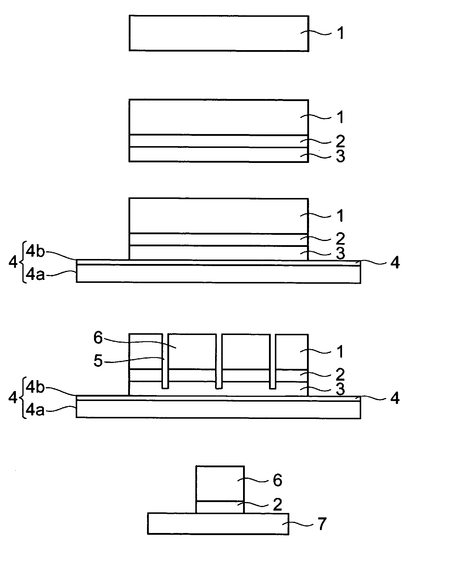
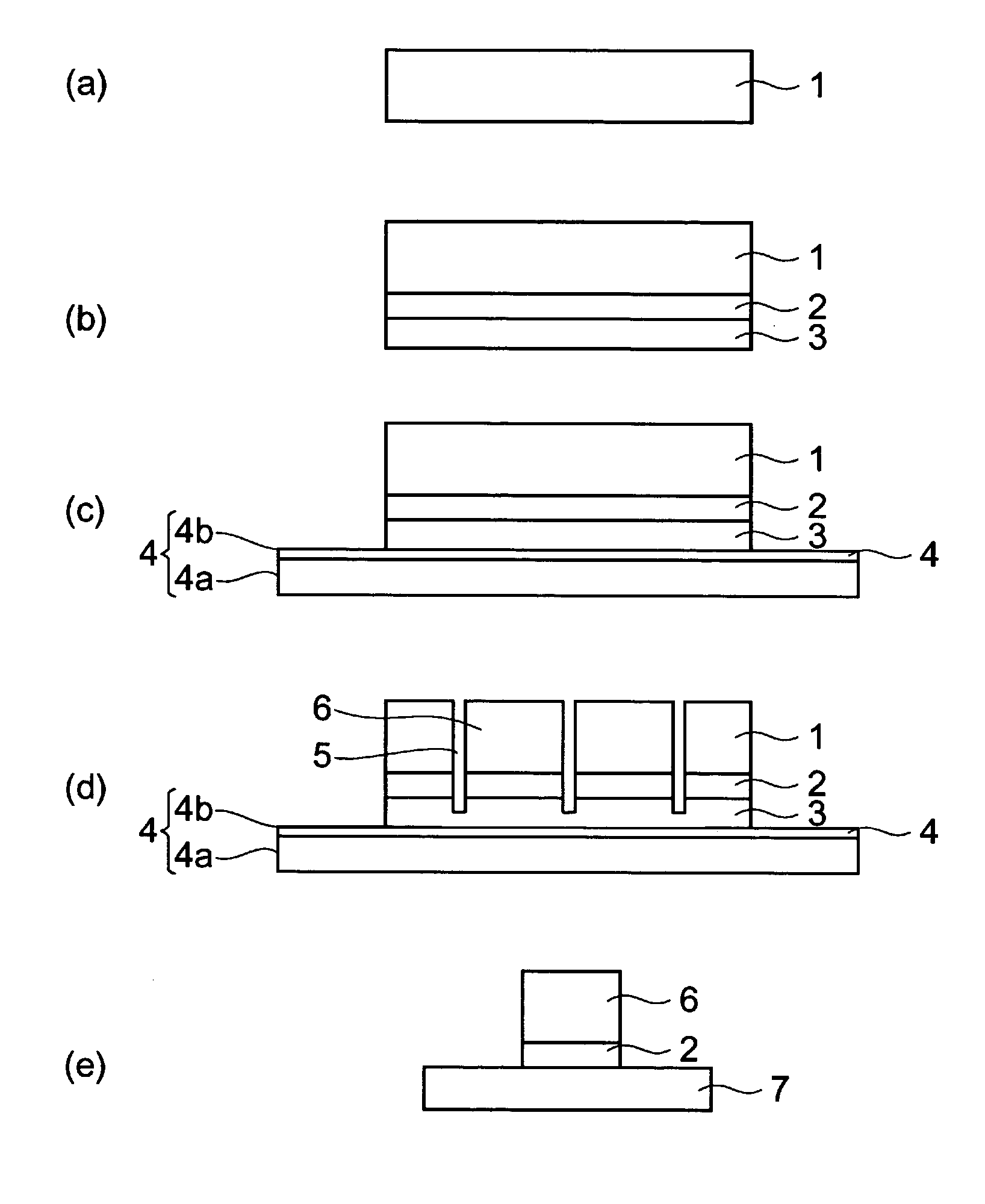
[0115] Hereinafter, on the basis of FIG. 3, an IC-chip mounting method according to a third embodiment of the present invention will be described. FIG. 3 is an explanatory view illustrating a wafer finishing process, an adhesive material attaching process, an IC-chip separating process and a mounting process, in an electronic member fabricating method according to the third embodiment of the present invention. The same components as those in the prior art are designated by the same reference symbols.

[0116] First, the wafer finishing process of FIG. 3(a) is the same as that in the prior art and description thereof is omitted herein.

[0117] In the adhesive material attaching process illustrated in FIG. 3(b), a film-type adhesive material 2 which has been formed in advance on a base film 3 is attached to a wafer 1 through a laminator, wherein the base film 3 also serves as a dicing film. After the completion of the attachment, no provisional curing is performed. It is preferable that ...

fourth and fifth embodiments

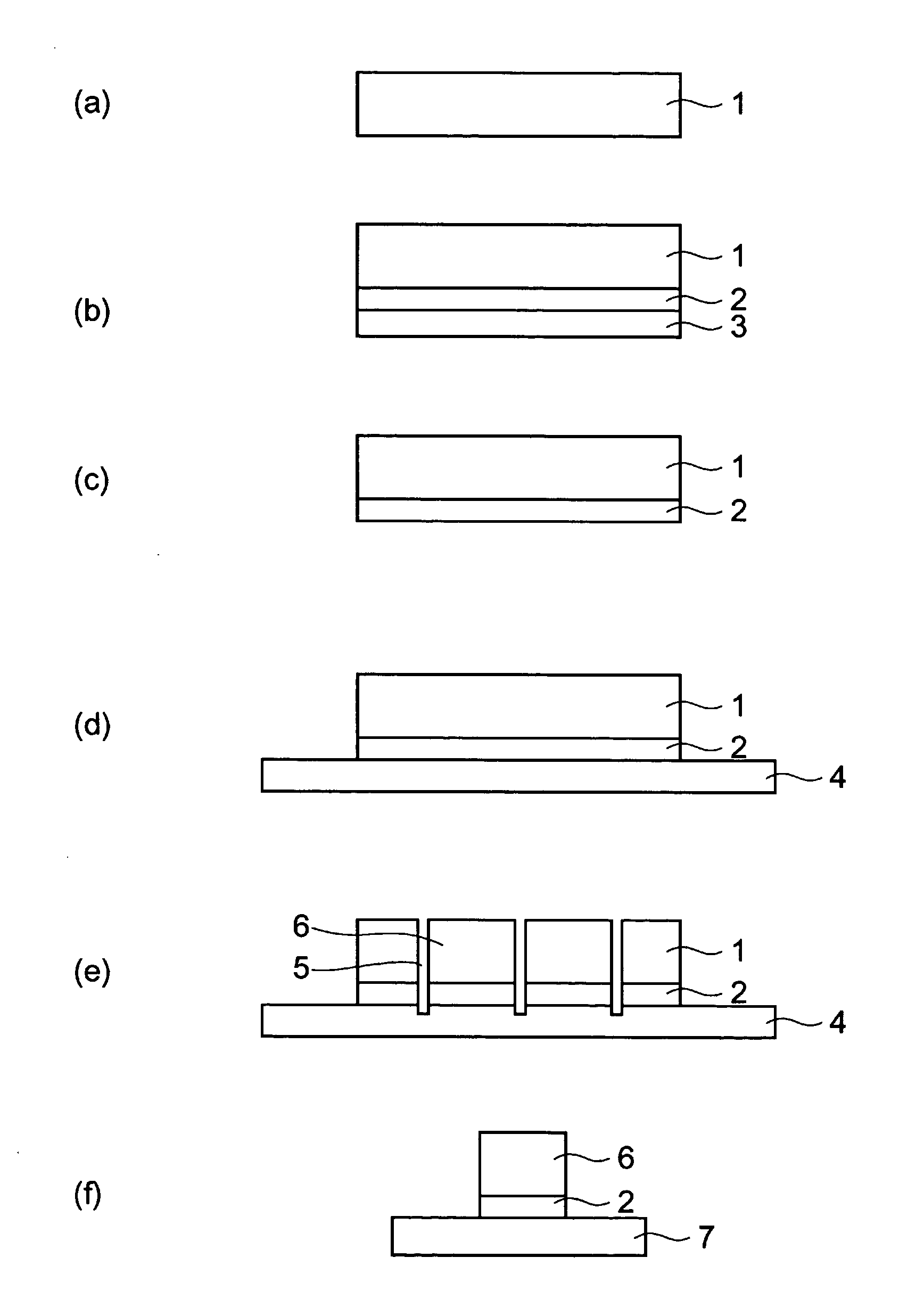
[0128] Hereinafter, on the basis of the drawings, an IC-chip mounting method according to the present invention will be described. FIG. 4 is a cross-sectional view of adhesive material-attached IC chips according to a fourth embodiment of the present invention. FIG. 5 is a cross-sectional view of another-adhesive material-attached IC chips according to a fifth embodiment of the present invention. The same components as those in the prior art are designated by the same reference symbols.

[0129]FIG. 4 illustrates adhesive material-attached IC chips which are fabricated by attaching, to a wafer, a material made of a base film and an adhesive material directly attached thereon, then attaching the base film to a dicing film and dicing them. A base film 23 is adhered to a dicing film 24, an adhesive material 22 is directly adhered to the base film 23 and IC chips 21 are adhered thereon. The IC chips 21 and the adhesive materials 22 are separated from the adjacent IC chips and adhesive mat...

first example

[0142] A material made of a PET film and an adhesive material with a thickness of 25 micrometers attached thereon was laminated on an 8-inch wafer with a thickness of 200 micrometers, at 80° C., with a pressure of 4 kgf (4×10⁵ Pa), wherein the adhesive material has a viscosity of 20000 Pa·s at 80° C. and also has a reaction starting temperature of 100° C. At this time, inspections were conducted for warpage of the wafer and voids between the wafer and the adhesive material (a microscope with a magnification of 50 times). There was observed no wafer warpage or void which would be problematic during the subsequent processes. Thereafter, it was laminated on a dicing film, and the wafer and the adhesive material were diced into squares having a chip size of 10-millimeter-square. At this time, inspections were conducted for burrs on the adhesive material and scatters of chips. There was found no problem in terms of burrs and chip scatters. Thereafter, IC chips were picked up from the sur...


PUM


Abstract

The present invention includes: an adhesive material attaching process for attaching a wafer to a thermoseffing adhesive material provided on a base film; a dicing-film attaching process for attaching the base film to a dicing film; an IC-chip separating process for cutting the wafer and the thermosetting adhesive material to divide them into IC chips; and a mounting process for attaching, to a carrier, the IC chips having the thermosetting adhesive material attached thereto; wherein the thermosetting adhesive material has a viscosity of 20000 Pa·s or less at the attaching temperature during the adhesive material attaching process.

Description

TECHNICAL FIELD [0001] The present invention relates to a method for fabricating an electronic member by forming an adhesive-applied IC chip from a wafer and then fixing it to a carrier and relates to the IC chip with adhesive material. BACKGROUND ART [0002] There is a conventional fabricating method which employs a wafer fixing member constituted by a thermosetting adhesive material, a dicing film and an ultraviolet curing adhesive placed therebetween (refer to, for example, Patent Document 1). [0003] Hereinafter, with reference to FIG. 6, a conventional electronic member fabricating method will be described. In a wafer finishing process illustrated in FIG. 6(a), devices are formed in or on a wafer 1. [0004] In a process for attaching an adhesive material including an ultraviolet curing adhesive illustrated in FIG. 6(b), a thermosetting adhesive material 8 is attached to the wafer 1. Thereafter, the thermosetting adhesive material 8 is semi-cured at 150° C. for 30 seconds, in order...

Claims


Application Information

Patent Timeline
IPC IPC(8): H01L21/58H01L23/12H01L21/301H01L21/52H01L21/68H01L21/78
CPCH01L21/6835H01L21/6836H01L21/78H01L24/27H01L24/83H01L2221/68327H01L2221/68331H01L2224/274H01L2224/83191H01L2224/83855H01L2924/01004H01L2924/01005H01L2924/01013H01L2924/01047H01L2924/07802H01L2924/10157H01L2924/14H01L2224/2919H01L2924/01006H01L2924/01033H01L2924/0665H01L2924/00H01L24/29H01L2224/94H01L2924/15787H01L2924/181
Inventor TAKAHASHI, ATSUSHIISHIDA, YOSHIHIRO
Owner NAGASE & COMPANY
Why Eureka
Try Eureka