Semiconductor memory

a technology of semiconductor memory and semiconductor chips, applied in information storage, static storage, digital storage, etc., can solve problems such as interference, and achieve the effect of improving frequency characteristics

Inactive Publication Date: 2006-06-15
SOCIONEXT INC
View PDF4 Cites 21 Cited by
  • Summary
  • Abstract
  • Description
  • Claims
  • Application Information

AI Technical Summary

Benefits of technology

[0009] An object of the present invention is providing a semiconductor memory device having a plurality of ports, capable of ensuring data read processing even when interference occurs between ports accessing the same row address simultaneously and one of the interfering access operations is read operation that is easily affected by the other access operation causing a longer processing time at the occurrence of processing overlap.
[0010] To attain the above object, according to the present invention, when the same row address is selected with access from a plurality of ports, adjustment may be made for the timing of output of activation signals for activating access transistors that connect bit lines to a memory cell. That is, while access from the first port is underway, access from the second port may be made causing the possibility of occurrence of interference due to the access from the second port. In such a case, a signal based on a control signal output from a control circuit of the first port for memory access is also sent to a control circuit of the second port that is to make access simultaneously, to thereby cause a delay in the control of the second port so that the access transistor for the second port be prevented from being activated simultaneously. In other words, the output timing of the activation signal is controlled.

Problems solved by technology

That is, while access from the first port is underway, access from the second port may be made causing the possibility of occurrence of interference due to the access from the second port.

Method used


Image

  • Semiconductor memory
  • Semiconductor memory
  • Semiconductor memory

Examples


embodiment 1

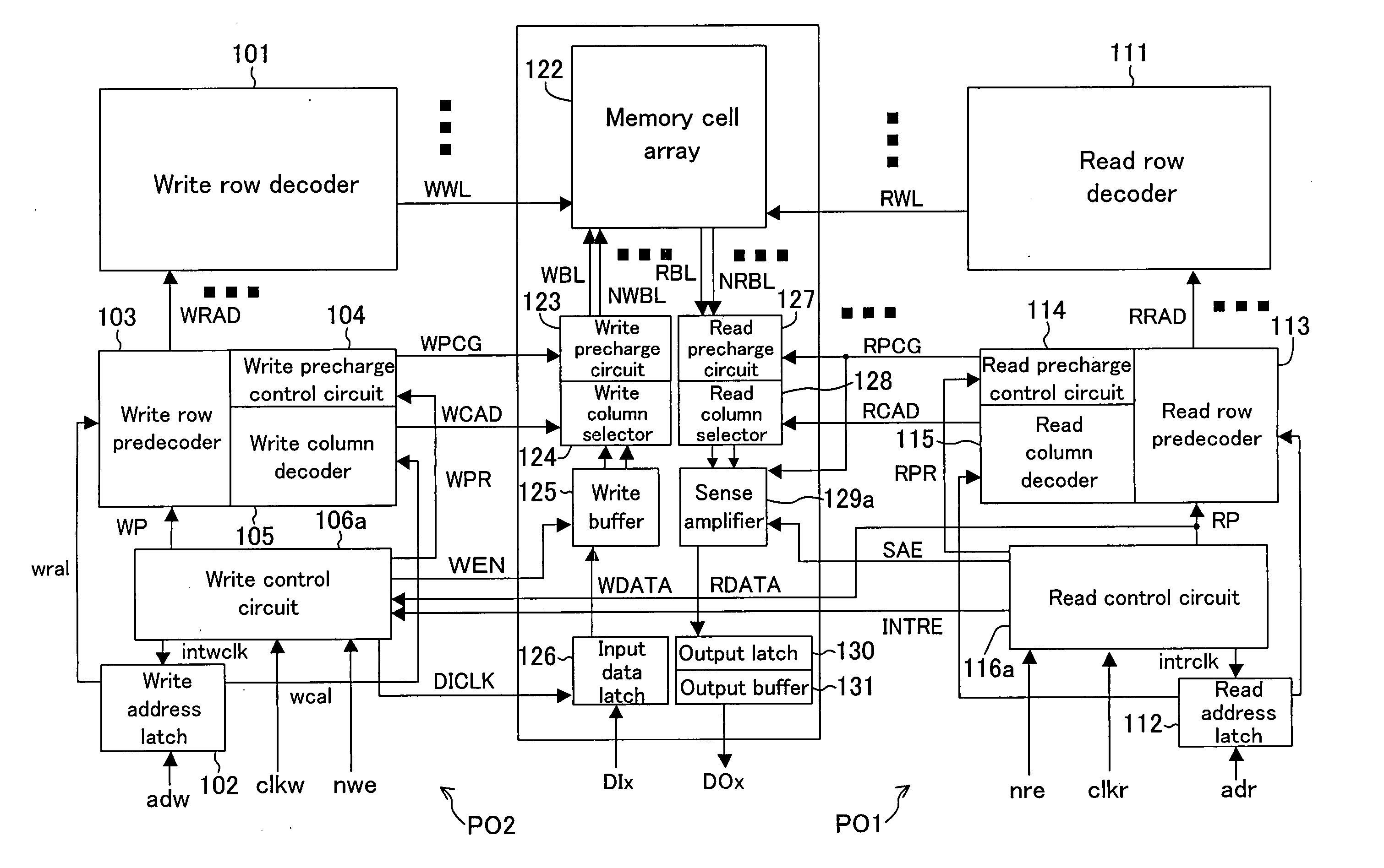
[0065]FIG. 1 shows the entire configuration of a semiconductor memory device of Embodiment 1 of the present invention.

[0066] The dual-port memory shown in FIG. 1 is a predecode type memory, in which a memory cell array 122 is connected with a write row decoder 101 via write word lines WWL, connected with a read row decoder 111 via read word lines RWL, connected with a write precharge circuit 123 via write bit line pairs WBL / NWBL, and connected with a read precharge circuit 127 via read bit line pairs RBL / NRBL.

[0067] The write row decoder 101 receives write row predecode signals WRAD from a write row predecoder 103. The write row predecoder 103 receives a write row address latch signal (write row address information) wral from a write address latch 102 and a write word line pulse signal WP from a write control circuit 106a. The read row decoder 111 receives read row predecode signals RRAD from a read row predecoder 113. The read row predecoder 113 receives a read row address latch ...

embodiment 2

[0104] Embodiment 2 of the present invention will be described with reference to the relevant drawings. FIG. 9 is a block diagram of a dual-port memory of Embodiment 2, which is different from the dual-port memory of FIG. 1 in that the sense amplifier startup signal SAE output from the read control circuit 116a to the sense amplifier 129a for starting the sense amplifier 129a is also sent to a write control circuit 106b, and that the output timing of the write activation signal is controlled with the signal SAE.

[0105] The write control circuit 106b in this embodiment is the same as the write control circuit 106a in Embodiment 1 shown in FIG. 8, except that the sense amplifier startup signal SAE is input in place of the read word line pulse signal RP.

[0106] In Embodiment 2 of the present invention, when receiving the sense amplifier startup signal (first control signal) SAE, the write control circuit 106b sequentially outputs the write precharge startup signal WPR (“L” pulse), the ...

embodiment 3

[0109] Embodiment 3 of the present invention will be described with reference to the relevant drawings. FIG. 10 is a block diagram of a dual-port memory of this embodiment, which is different from the dual-port memory of Embodiment 1 shown in FIG. 1 in that a sensing confirmation signal ASA (first control signal) output from a sense amplifier 129b when the sense amplifier 129b detects sense amplification is input into a write control circuit 106c, in place of the read word line pulse signal RP.

[0110]FIG. 15 shows a write control circuit 106c in this embodiment, in which the sensing confirmation signal ASA is sent via an inverter I41 to one of the input terminals of the 3-input NAND circuit 3NA2, in place of the read word line pulse signal RP that is input into the write control circuit 106a shown in FIG. 8.

[0111]FIG. 11 shows the sense amplifier 129b in this embodiment that detects sense amplification by NAND-operating a read data line pair RDBUS / NRDBUS and generates the sensing c...


PUM


Abstract

In a multiport memory, in the event of simultaneous read / write operation for the same row address, a read word line pulse signal, output from a read control circuit for memory access based on an externally supplied read enable signal and read clock signal, is input into a write control circuit, to delay start of the write operation until termination of the read operation. This can delay the timing of activating a write word line by a write row decoder behind the timing of activating a read word line by a read row decoder, to allow the read operation first followed by the write operation. Therefore, since the read operation is performed while the write word line being kept closed, the trouble of data processing becoming uncertain due to addition of the load of a write bit line to a read bit line can be prevented.

Description

CROSS-REFERENCE TO RELATED APPLICATIONS [0001] This application relates to Japanese Patent Application No. 2004-319351 filed in Japan on Nov. 2, 2004, the entire contents of which are hereby incorporated by reference. BACKGROUND OF THE INVENTION [0002] The present invention relates to a multiport semiconductor memory device. [0003]FIG. 22 shows a conventional dual-port RAM, in which one cycle is time-divided into two to provide access time periods dedicated to A port 12 and B port 13. Specifically, in the former half of the cycle, a chip enable signal / CEA for the A port 12 is put in a low level (selected) to allow access with an address ADRA, while in the latter half of the cycle, a chip enable signal / CEB for the B port 13 is put in a low level (selected) to allow access with an address ADRB. Therefore, even if both ports 12 and 13 happen to access the same address for write in the same cycle, such access attempts will not conflict with each other ideally due to the time-division ...

Claims


Application Information

Patent Timeline
Patent Type & Authority Applications(United States)
IPC IPC(8): G11C8/00
CPCG11C8/16
Inventor KURUMADA, MAREFUSATERADA, YUTAKA
Owner SOCIONEXT INC
Why Eureka
Try Eureka