Optical semiconductor apparatus

a technology of optical semiconductor and optical semiconductor, applied in the direction of semiconductor devices, semiconductor/solid-state device details, electrical devices, etc., can solve the problems of increasing the number of components and the manufacturing cost, and achieve the effect of increasing the reliability of optical semiconductor apparatus

Active Publication Date: 2020-11-24
NIKKISO COMPANY
View PDF31 Cites 9 Cited by
  • Summary
  • Abstract
  • Description
  • Claims
  • Application Information

AI Technical Summary

Benefits of technology

[0006]In this background, one illustrative purpose of the present invention is to provide a technology for increasing the reliability of an optical semiconductor apparatus.
[0008]According to the embodiment, the active layer provided in the inner region is sealed by the seal ring and the sealing part provided in a shape of a frame in the outer region of the optical semiconductor device. Accordingly, the active layer, which needs be protected, is sealed without using a package substrate or a lid body for sealing the active layer by encircling the entirety of the optical semiconductor device. Accordingly, the number of components required for sealing is reduced and the manufacturing cost is lowered, while at the same time maintaining the reliability of sealing.

Problems solved by technology

An increase in the complexity of the sealing structure for protecting the device properly from an external environment leads to an increase in the number of components and the manufacturing cost.

Method used


Image

  • Optical semiconductor apparatus
  • Optical semiconductor apparatus
  • Optical semiconductor apparatus

Examples


Embodiment Construction

[0029]The invention will now be described by reference to the preferred embodiments. This does not intend to limit the scope of the present invention, but to exemplify the invention.

[0030]A detailed description will be given of embodiments of the present invention with reference to the drawings. Same numerals are used in the description to denote same elements and duplicate descriptions are omitted as appropriate. To facilitate the understanding, the relative dimensions of the constituting elements in the drawings do not necessarily mirror the relative dimensions in the actual apparatus.

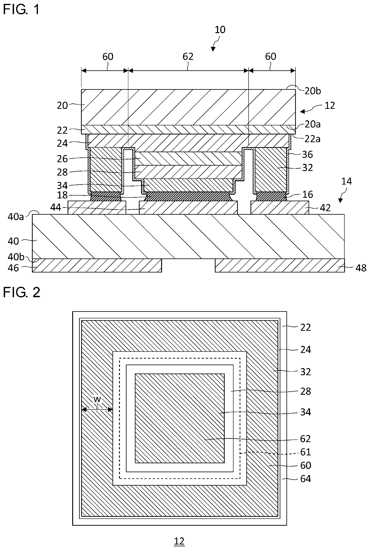
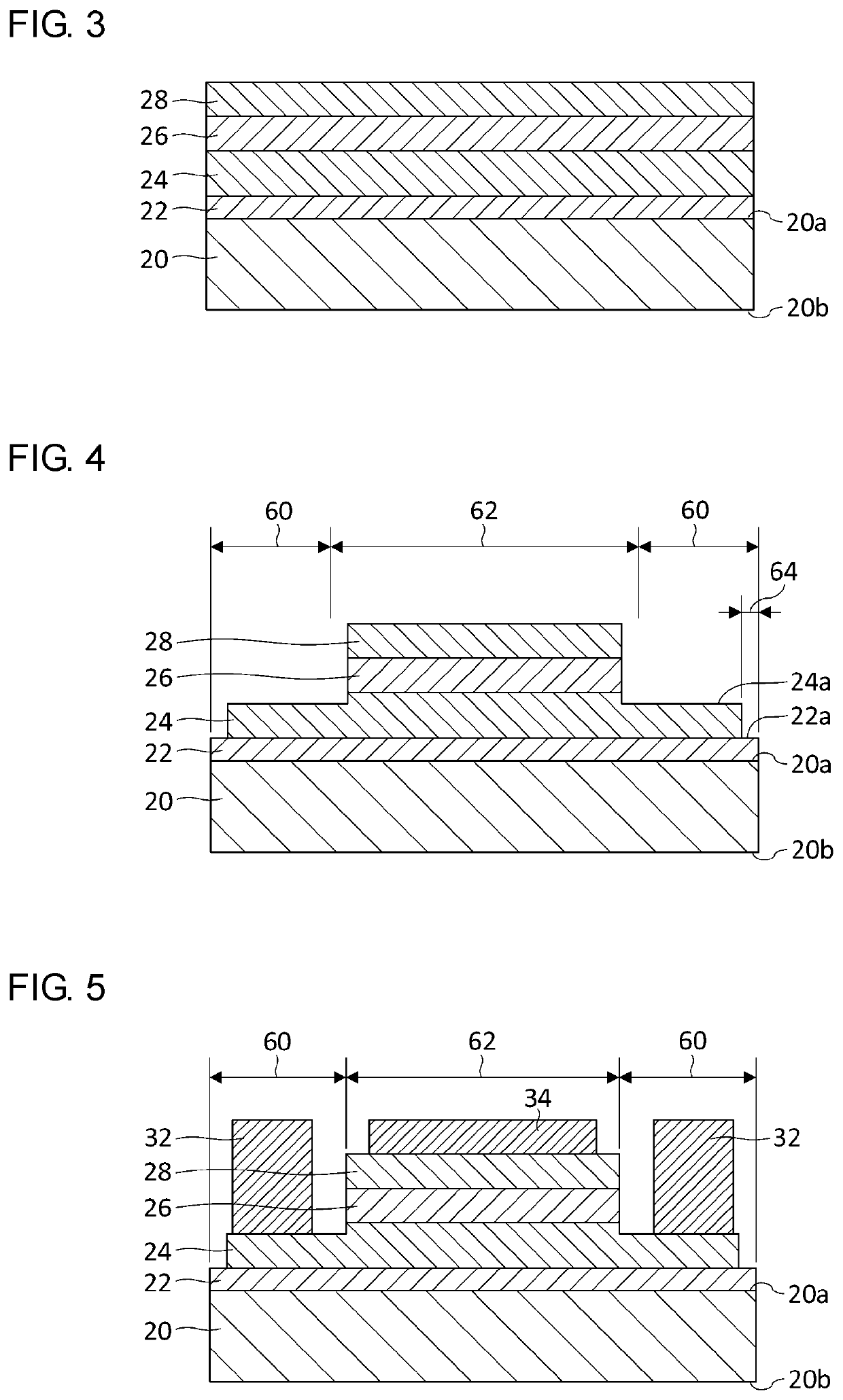
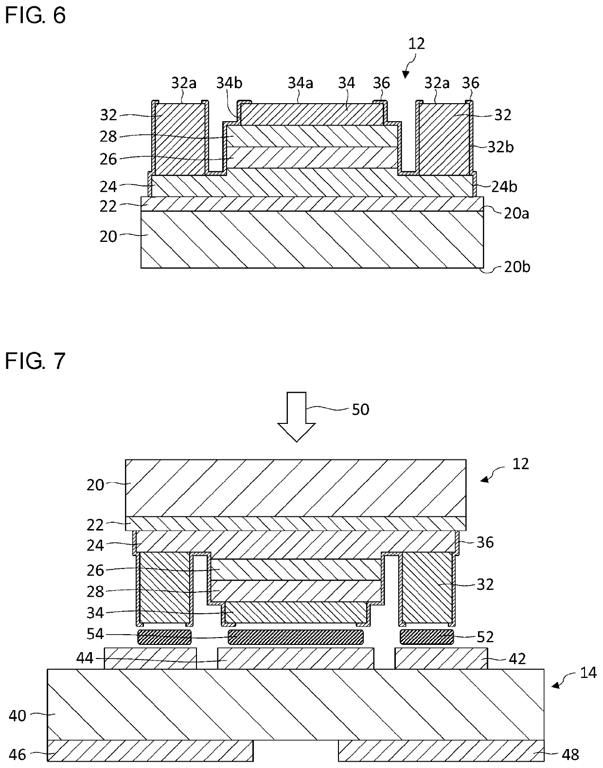
[0031]FIG. 1 is a cross-sectional view schematically showing an optical semiconductor apparatus 10 according to an embodiment, and FIG. 2 is a top view schematically showing an optical semiconductor device 12 of FIG. 1. The optical semiconductor apparatus 10 includes an optical semiconductor device 12, a package substrate 14, a sealing part 16, and a bonding part 18.

[0032]The optical semiconductor de...


PUM

PropertyMeasurementUnit
central wavelengthaaaaaaaaaa
band gapaaaaaaaaaa
thicknessaaaaaaaaaa

Abstract

An optical semiconductor apparatus includes: an optical semiconductor device including a translucent support substrate; a buffer layer on the support substrate, a seal ring in a frame shape provided in an outer region on the buffer layer, an active layer provided on an inner region of the buffer layer, and an electrode provided on the active layer. The optical semiconductor apparatus further including: a package substrate on which the optical semiconductor device is mounted; and a sealing part that seals a space between the seal ring and the package substrate.

Description

RELATED APPLICATION[0001]Priority is claimed to Japanese Patent Application No. 2016-237607, filed on Dec. 7, 2016, the entire content of which is incorporated herein by reference.BACKGROUND OF THE INVENTION1. Field of the Invention[0002]The present invention relates to optical semiconductor apparatuses, and, more particularly, to an optical semiconductor apparatus including an optical semiconductor device.2. Description of the Related Art[0003]Nowadays, semiconductor light emitting devices such as light emitting diodes and laser diodes that emit blue light have been in practical use. Development of light emitting devices that output deep ultraviolet light having a shorter wavelength has also been pursued. Deep ultraviolet light has high sterilization capability. Semiconductor light emitting devices capable of outputting deep ultraviolet light have therefore attracted attention as a mercury free sterilization light source in medical and food processing fields.[0004]A light emitting ...

Claims


Application Information

Patent Timeline
Patent Type & Authority Patents(United States)
IPC IPC(8): H01L33/62H01L33/38H01L23/02H01L23/00H01L33/32H01L33/48H01L33/54
CPCH01L33/38H01L23/02H01L24/29H01L24/32H01L33/62H01L24/33H01L2224/29171H01L2224/29144H01L2224/32225H01L33/32H01L2224/29083H01L2224/16225H01L33/486H01L2224/29166H01L2224/29111H01L33/54H01L2224/29169H01L2933/0016H01L2933/0066
Inventor NIIZEKI, SHOICHIICHINOKURA, HIROYASU
Owner NIKKISO COMPANY
Why Eureka
Try Eureka