Optical element

a technology of optical elements and optical elements, applied in the field of optical elements, can solve problems such as the possibility of layer exfoliation, and achieve the effect of improving the reliability of optical elements

Inactive Publication Date: 2008-03-11
SEIKO EPSON CORP
View PDF4 Cites 4 Cited by
  • Summary
  • Abstract
  • Description
  • Claims
  • Application Information

AI Technical Summary

Benefits of technology

[0007]In accordance with an advantage of some aspects of the present invention, the reliability of optical elements can be improved against environmental changes such as changes in temperature, humidity and the like.
[0009]According to the embodiment described above, the first and second protection layers are composed of a material harder than the resin layer, such that these protection layers act to press the resin layer from both sides thereof whereby deformation of the resin layer can be effectively prevented. Also, the first and second protection layers can improve adhesion and moisture-resistant property, such that exfoliation of the resin layer can be effectively prevented.
[0013]By this, for example, harmful effects that may be caused by unintended oxidation of the columnar section due to infiltration of moisture content can be prevented. Also, adhesion strength between the resin layer and the columnar section is improved, and thus the resin layer can be effectively prevented from peeling off.
[0017]By this, deformation of the resin layer can be more effectively prevented.
[0019]By this, exfoliation and oxidation of the electrode can be better prevented.
[0021]By this, deformation of the resin layer can be more effectively prevented.

Problems solved by technology

Also, because resin (for example, a high polymer material such as polyimide resin) has a few permeability to moisture, there is a possibility that exfoliation of layers may occur due to absorption of moisture at an interface between the resin layer and an electrode or between the resin layer and a substrate.

Method used


Image

  • Optical element
  • Optical element
  • Optical element

Examples


Embodiment Construction

[0043]Exemplary embodiments of the invention are described below with reference to the accompanying drawings.

[0044]A. Optical Element

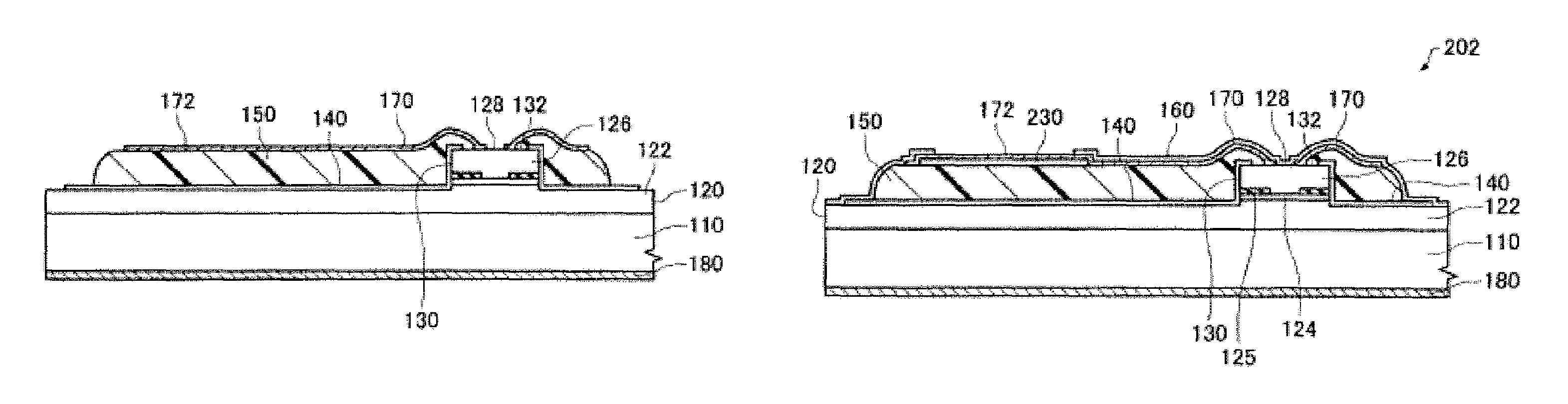
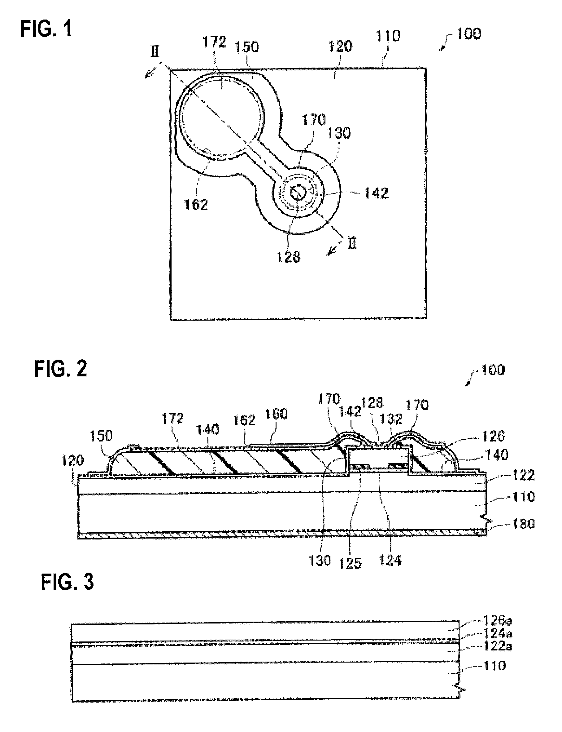
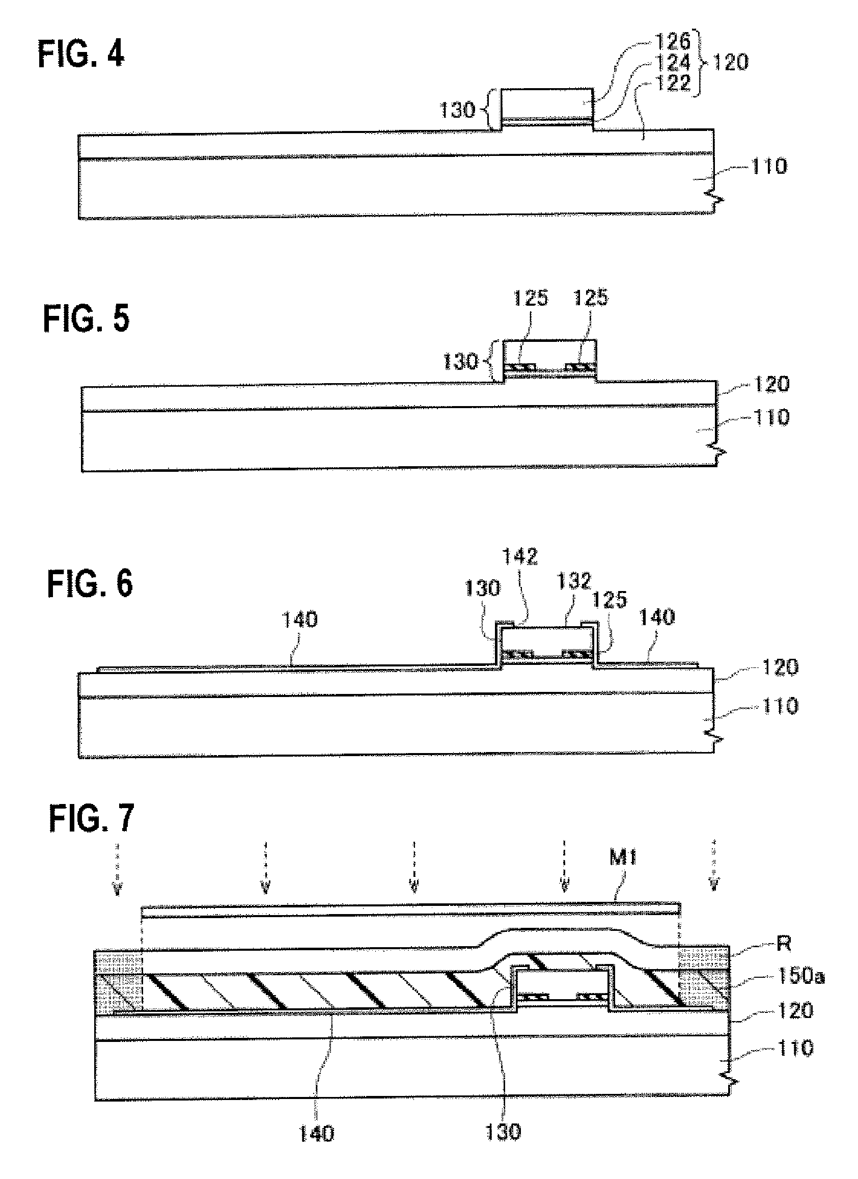
[0045]FIG. 1 is a plan view of an optical element in accordance with an embodiment of the invention, and FIG. 2 is a cross-sectional view taken along a line II-II in FIG. 1.

[0046]The optical element 100 includes a substrate 110, an element section 120 (including a columnar section 130), a first protection layer 140, a resin layer 150, a second protection layer 160, an electrode 170, and another electrode 180. In the present embodiment, an example in which the optical element 100 is a surface-emitting type device (surface-emitting type semiconductor laser) is described.

[0047](A-1) First, the substrate 110 and the element section 120 are described.

[0048]The substrate 110 is a semiconductor substrate (for example, an n-type GaAs substrate). The element section 120 is formed on the substrate 110. The substrate 110 and the element section 120 may have the s...


PUM

PropertyMeasurementUnit
temperaturesaaaaaaaaaa
circumferenceaaaaaaaaaa
areaaaaaaaaaaa

Abstract

An optical element includes a substrate, a columnar section that is formed above the substrate and has an upper surface for light emission or light incidence, a first protection layer formed above the substrate in a region including at least a circumference of the columnar section, a resin layer formed above the first protection layer, a second protection layer formed above the resin layer, and an electrode that is electrically connected to the upper surface of the columnar section, wherein the first and second protection layers are composed of a material harder than the resin layer.

Description

[0001]The entire disclosure of Japanese Patent Application No. 2005-159517, filed May 31, 2005 is expressly incorporated by reference herein.BACKGROUND[0002]1. Technical Field[0003]The present invention relates to optical elements.[0004]2. Related Art[0005]An optical element may have a structure that includes a substrate, a columnar section that is formed above the substrate for light emission or light incidence, a resin layer formed around the columnar section, and an electrode electrically connected to an upper surface of the columnar section. For example, Japanese Laid-open Patent Application JP-A-2004-31633 describes a structure in which an additional protective film is provided between a substrate and a polyimide protective film to thereby prevent the polyimide protective film from peeling off.[0006]It is noted that resin is relatively soft, and would likely expand or contract according to changes in temperature. Therefore it is important to prevent its deformation. Also, becau...

Claims


Application Information

Patent Timeline
Patent Type & Authority Patents(United States)
IPC IPC(8): H01L33/00H01L21/00H01L23/29H01L23/31H01S5/022
CPCB82Y20/00H01L24/82H01L31/02161H01L33/38H01L33/62H01S5/0425H01L24/18H01L2224/82102H01L2224/18H01L2224/76155H01L2924/01012H01L2924/01013H01L2924/01015H01L2924/0103H01L2924/01032H01L2924/01078H01L2924/01079H01L2924/10329H01L2924/10336H01L2924/30105H01S5/18311H01S5/2213H01S5/3432H01S2301/176H01L2924/01005H01L2924/01006H01L2924/01033H01L2924/12041H01L24/24H01L2224/73267H01L2924/3512H01S5/04254
Inventor NAGAWA, MICHIFUMIKANEKO, TSUYOSHISATO, ATSUSHI
Owner SEIKO EPSON CORP
Why Eureka
Try Eureka