Device substrate

a technology of device substrate and substrate, which is applied in the direction of identification means, semiconductor devices, instruments, etc., can solve the problems of difficult to meet consumer demands for new products, appearance variability of shaped display panels can attract the attention of consumers, and produced shaped display panels may not operate normally in most cases, so as to improve the yield of a cutting process

Active Publication Date: 2021-01-05
AU OPTRONICS CORP
View PDF9 Cites 0 Cited by
  • Summary
  • Abstract
  • Description
  • Claims
  • Application Information

AI Technical Summary

Benefits of technology

[0005]The present invention provides a device substrate, which can improve the yield of a cutting process.
[0009]One of the objects of the present invention is to increase the yield of a cutting process of a device substrate.

Problems solved by technology

With the development of science and technology, simply improving the display quality of display panels has made it difficult to meet consumer demands for new products.
The appearance variability of the shaped display panel can attract the attention of consumers.
However, if a driving circuit of the large panel is damaged in a cutting process, the produced shaped display panel may not operate normally in most cases.

Method used


Image

  • Device substrate
  • Device substrate
  • Device substrate

Examples


Embodiment Construction

[0035]It should be understood that although terms such as “first”, “second”, and “third” in this specification may be used for describing various elements, components, areas, layers, and / or parts, the elements, components, areas, layers, and / or parts are not limited by such terms. The terms are only used to distinguish one element, component, area, layer, or part from another element, component, area, layer, or part. Therefore, the “first element”, “component, “area”, “layer”, or “part” described below may also be referred to as a second element, component, area, layer, or part without departing from the teachings of the present invention.

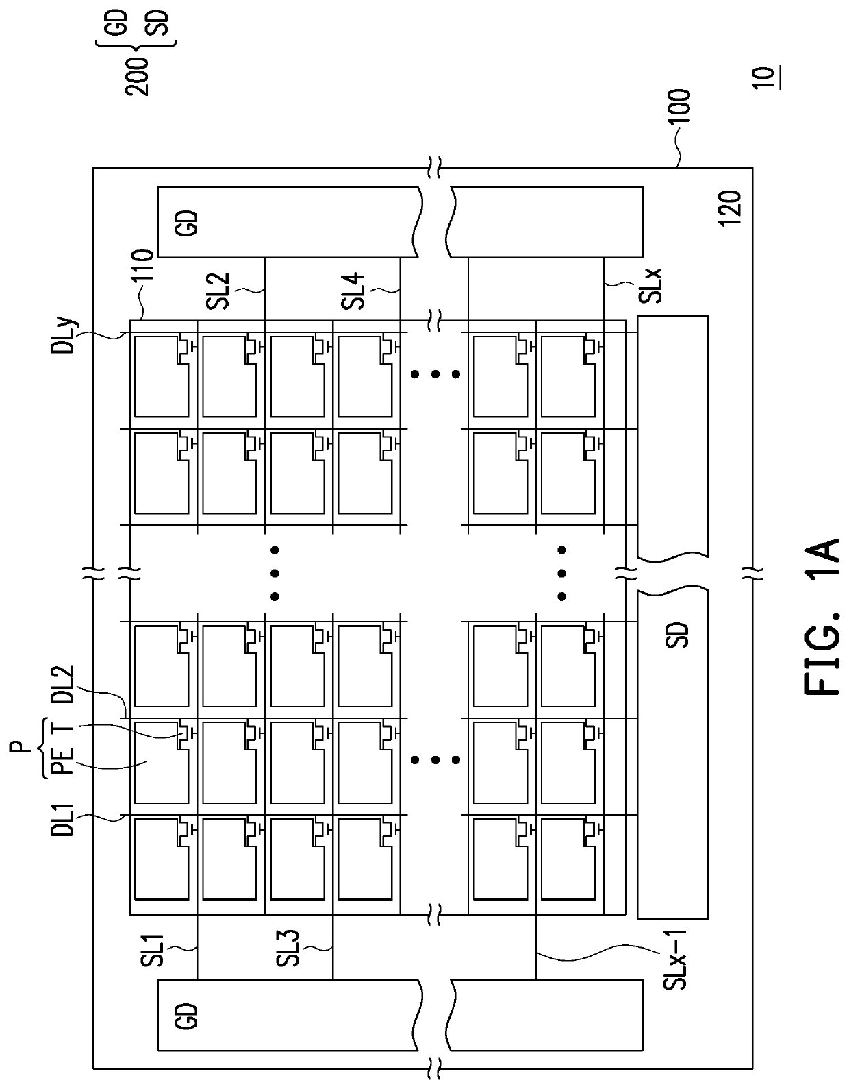
[0036]FIG. 1A is a schematic top view of a device substrate according to an embodiment of the present invention.

[0037]Referring to FIG. 1A, a device substrate 10 includes a substrate 100, a driving circuit 200, a plurality of scan lines SL1-SLx, a plurality of data lines DL1-DLy, and a plurality of pixel structures P. The substrate 100 has an activ...


PUM


Abstract

A device substrate includes a substrate, a first output circuit, a first auxiliary circuit, and a first backup circuit. The substrate has an active area and a peripheral area located on at least one side of the active area. A cutting path overlaps the active area and the peripheral area. The first output circuit is located on the peripheral area. The first auxiliary circuit is located on the peripheral area. The first auxiliary circuit overlaps the cutting path. The first backup circuit is located on the peripheral area and is electrically connected with the first auxiliary circuit. The first auxiliary circuit and the first backup circuit are pull-down circuits or are pull-up circuits. The shortest distance between the first backup circuit and the cutting path is from 125 microns to 300 microns.

Description

CROSS-REFERENCE TO RELATED APPLICATION[0001]This application claims the priority benefit of Taiwan application serial no. 108120866, filed on Jun. 17, 2019. The entirety of the above-mentioned patent application is hereby incorporated by reference herein and made a part of this specification.BACKGROUNDTechnical Field[0002]The present invention relates to a device substrate, and more particularly, to a device substrate having a backup circuit.Description of Related Art[0003]With the development of science and technology, simply improving the display quality of display panels has made it difficult to meet consumer demands for new products. In order to increase the attractiveness of the products, various manufacturers are committed to the development of a shaped display panel. The shaped display panel is different from conventional rectangular display panels. The appearance variability of the shaped display panel can attract the attention of consumers.[0004]Currently, a large panel is ...

Claims


Application Information

Patent Timeline
Patent Type & Authority Patents(United States)
IPC IPC(8): H01L27/12G09G3/20
CPCH01L27/1218H01L27/124G09G3/20G09G2300/0408G09G2310/0267G09G2310/08G09F9/30G09F9/302G09G2330/08G09G3/006G09G2310/0286G09G2300/0426
Inventor HUANG, PAO-YUCHEN, KUAN-YU
Owner AU OPTRONICS CORP
Why Eureka
Try Eureka