Supercharge Your Innovation With Domain-Expert AI Agents!

Direct memory access (DMA) controller, device and method using a write control module for reorganization of storage addresses in a shared local address space

a controller and storage address technology, applied in the direction of memory adressing/allocation/relocation, instruments, computing, etc., can solve the problems of inability to anticipate the reorganization of data at the source, excessively large amounts of metadata in addition to actual data transmission, etc., and achieve the effect of reducing computing tim

Active Publication Date: 2021-02-02
COMMISSARIAT A LENERGIE ATOMIQUE ET AUX ENERGIES ALTERNATIVES
View PDF14 Cites 0 Cited by
  • Summary
  • Abstract
  • Description
  • Claims
  • Application Information

AI Technical Summary

Benefits of technology

The patent describes a method to improve the efficiency of data processing by directly reorganizing the addresses of data being received, without the need for intermediary storage. This results in a reduction of memory space and processing time, and can thus save about a third of local memory space and cut computing time in half.

Problems solved by technology

But some processing is not capable of anticipating a reorganization of the data at the source, meaning that this must be done upon receipt.
But for complex reorganizations, such a method is likely to lead to transmissions of excessively large quantities of metadata in addition to the actual data.

Method used


Image

  • Direct memory access (DMA) controller, device and method using a write control module for reorganization of storage addresses in a shared local address space
  • Direct memory access (DMA) controller, device and method using a write control module for reorganization of storage addresses in a shared local address space
  • Direct memory access (DMA) controller, device and method using a write control module for reorganization of storage addresses in a shared local address space

Examples


Embodiment Construction

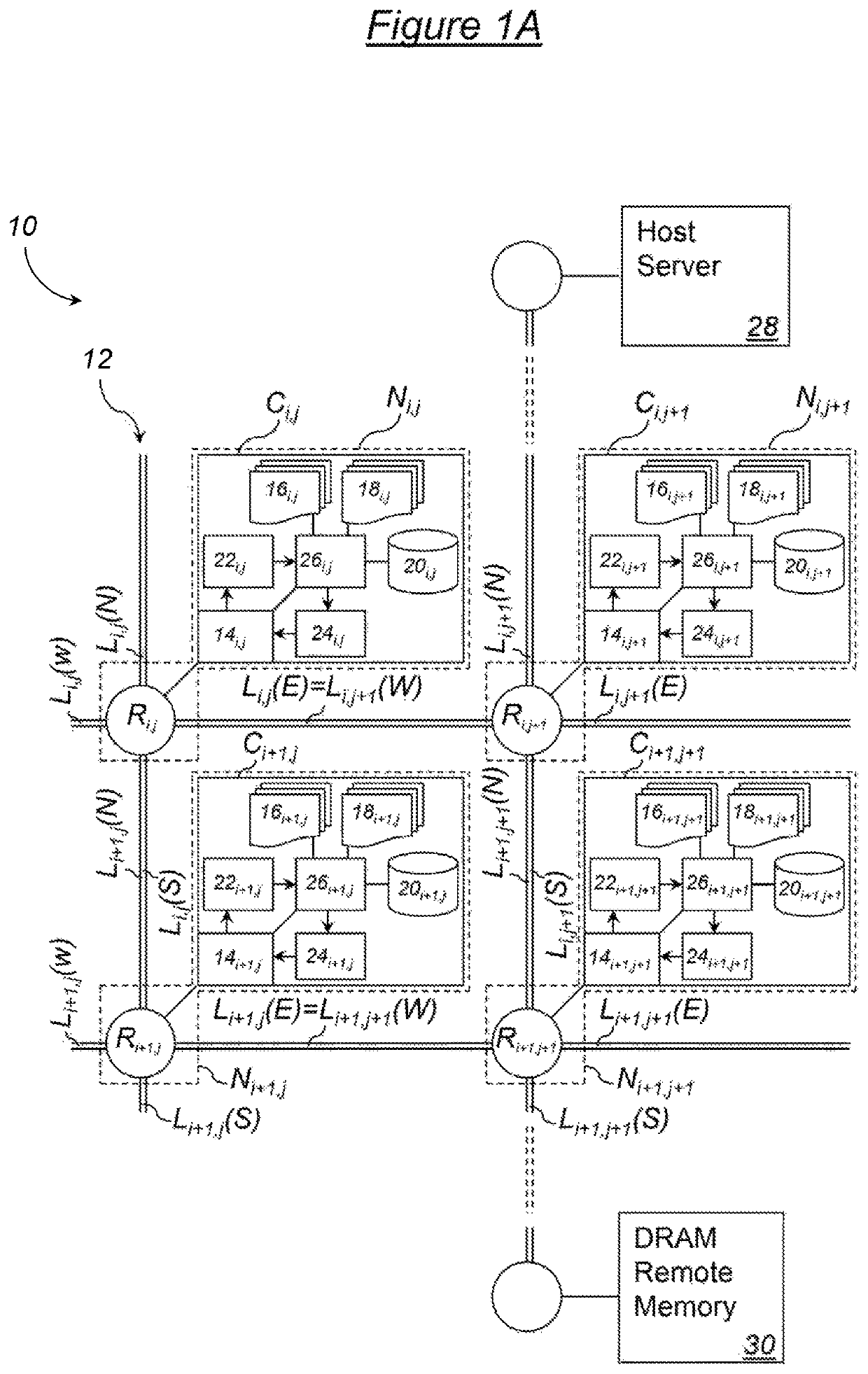
[0055]Data processing device 10 shown in FIG. 1A comprises a network on a chip, partially shown. This network on a chip, made in the form of an integrated circuit, consists of a plurality of nodes arranged in a matrix and interconnected with each other by bidirectional links oriented in four different matrix directions, North (N), South (S), West (W), and East (E). The links allow data packets to be transmitted from one node to another and form an interconnection network 12.

[0056]In the example of FIG. 1A, only four nodes are shown without any limiting intent, indicated as Ni,j, Ni,j+1, Ni+1,j, and Ni+1,j+1. Four bidirectional links Li,j(N), Li,j(S), Li,j(W), and Li,j(E) go from node Ni,j in the four directions mentioned above. Four bidirectional links Li,j+1(N), Li,j+1(S), Li,j+1(W), and Li,j+1(E) go from node Ni,j+1 in the four directions mentioned above. Four bidirectional links Li+1,j(N), Li+1,j(S), Li+1,j(W), and Li+1,j(E) go from node Ni+1,j in the four directions mentioned ab...


PUM


Abstract

A direct memory access controller, configured to be used in a computing node of a system on chip (SoC), includes: (1) an input buffer for receiving packets of data coming from an input / output interface of the computing node; (2) a write control module for controlling writing of data extracted from each packet to a local memory of the computing node shared by at least one processor other than the direct memory access controller; and (3) an arithmetic logic unit for executing microprograms. The write control module is configured to control the execution by the arithmetic logic unit of at least one microprogram including instruction lines for arithmetic and / or logical calculation concerning only storage addresses for storing the data received by the input buffer for a reorganization of the data in the shared local memory. Optionally, at least one microprogram may be stored in a register, and at least two operating modes (e.g., restart mode and pause mode) of the at least one microprogram stored in the register may be configurable. Exemplary microprograms can (1) provide image processing parameters including sizes of columns of image blocks, (2) provide image processing parameters including numbers of successive pieces of data to be processed which are to be written to successive addresses in the shared local memory, and (3) utilize a sequential write mode and / or an absolute-offset write mode. Microprograms may be selected based on an identifier included in a header of each packet.

Description

[0001]The invention relates to a direct memory access controller to be placed in a computing node of a system on chip. It also relates to a data processing device of a network-on-chip in which each computing node includes such a direct memory access controller. It also relates to a data reception and storage method which can be implemented using such a direct memory access controller.BACKGROUND OF THE INVENTION[0002]Such a controller, termed a DMA (Direct Memory Access) controller, is generally used in a data processing device employing distributed processing requiring numerous data transfers between various computing nodes. The controller makes it possible to transfer data to be processed or already processed by a processor or accelerator of a computing node coming from or going to a peripheral, such as another computing node, a communication port, a hard drive, or any kind of memory. The transfer is made between the peripheral and a local memory placed as close as possible to the ...

Claims


Application Information

Patent Timeline
Patent Type & Authority Patents(United States)
IPC IPC(8): G06F12/10G06F13/28G06F12/1081
CPCG06F12/1081G06F13/28G06F2212/621G06F2213/0038G06F2213/28
Inventor DURAND, YVESBERNARD, CHRISTIAN
Owner COMMISSARIAT A LENERGIE ATOMIQUE ET AUX ENERGIES ALTERNATIVES
Features
  • R&D
  • Intellectual Property
  • Life Sciences
  • Materials
  • Tech Scout
  • Unparalleled Data Quality
  • Higher Quality Content
  • 60% Fewer Hallucinations
Learn More