Wiring substrate and display panel

a technology of wiring substrate and display panel, which is applied in the direction of printed circuits, instruments, optics, etc., can solve the problems of image irregularity and display panel appearan

Active Publication Date: 2021-02-23
SHARP KK
View PDF2 Cites 1 Cited by
  • Summary
  • Abstract
  • Description
  • Claims
  • Application Information

AI Technical Summary

Benefits of technology

[0019]According to one aspect of the present invention, a wiring substrate that can obtain uniform signals can be provided even when connection wires formed on a wiring substrate are overlappingly arranged. Also, a display panel that uses such a wiring substrate and that can obtain uniform signals is provided.

Problems solved by technology

However, when such connection wires are configured to have a multi-layer structure, for example, it has been found that a failure, such as image irregularity, occurs in the display panel.

Method used


Image

  • Wiring substrate and display panel
  • Wiring substrate and display panel
  • Wiring substrate and display panel

Examples


first embodiment

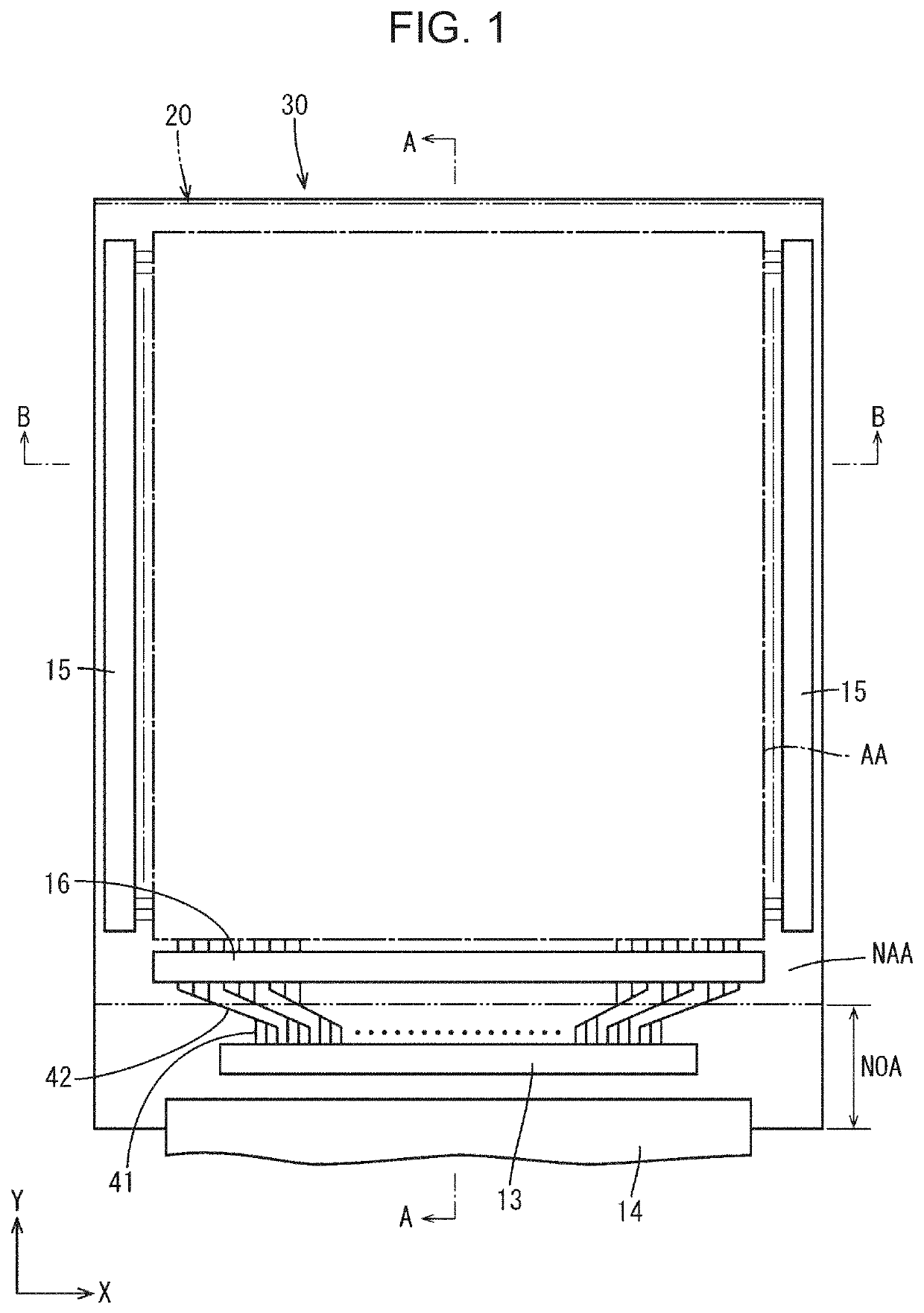
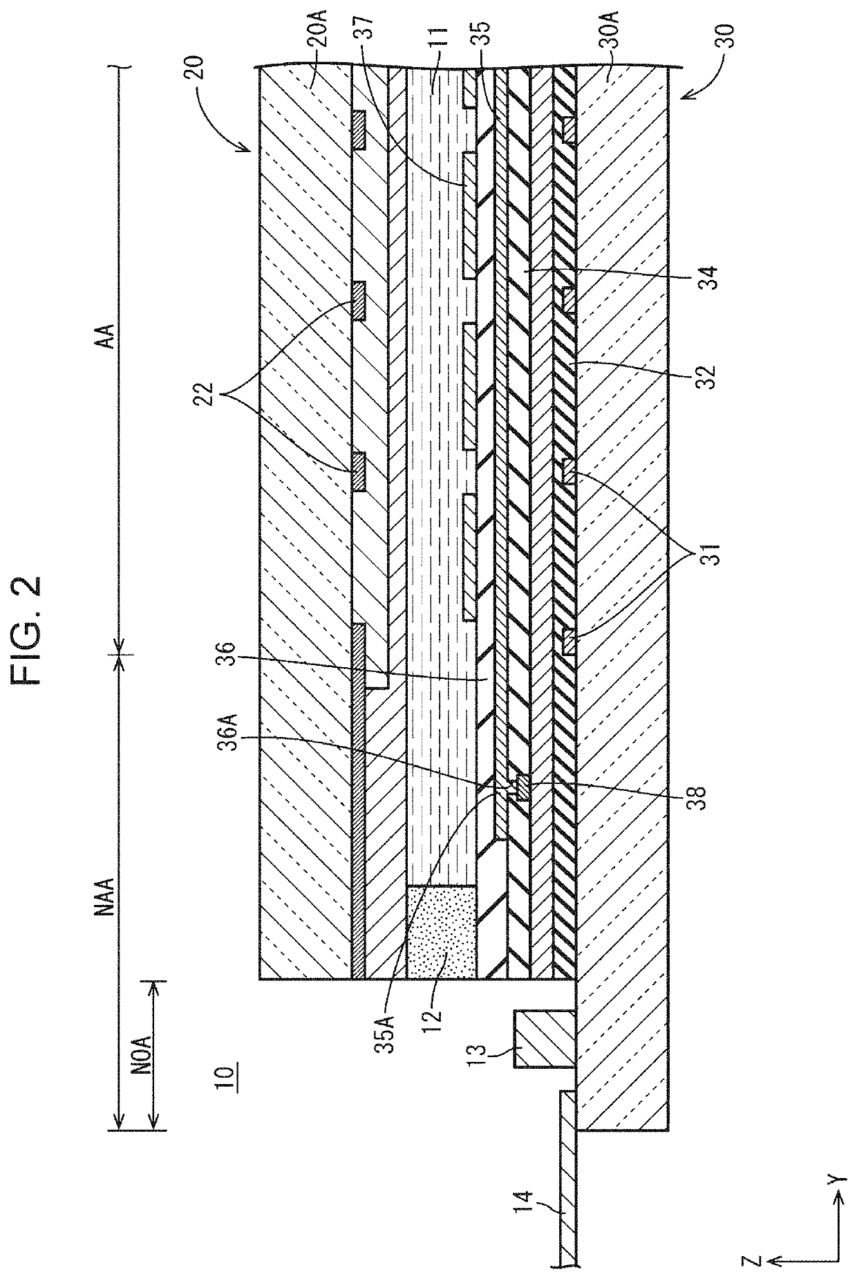
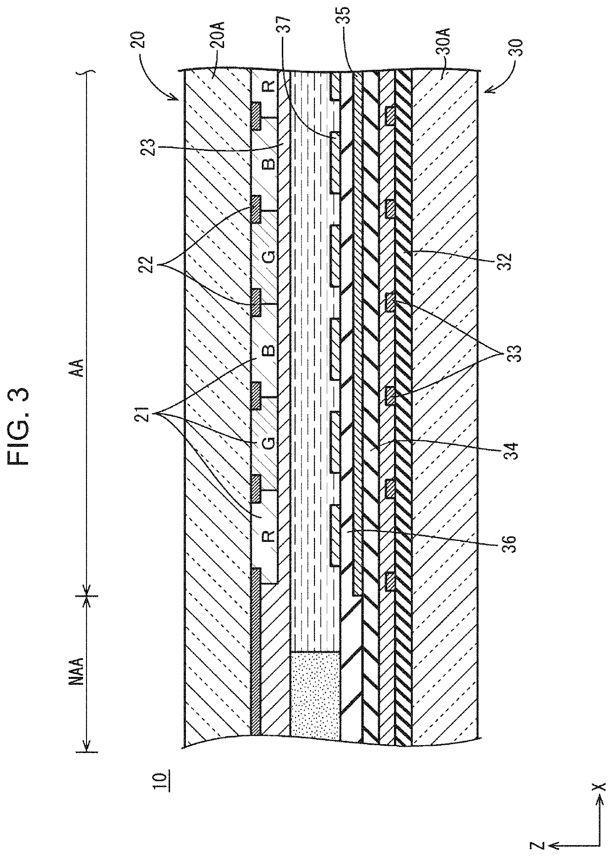
[0037]A liquid-crystal panel (one example of a display panel) 10 in a first embodiment will be described with reference to FIGS. 1 to 11. An X-axis, a Y-axis, and a Z-axis are illustrated in some of the drawings, and the directions of the axes are depicted as corresponding to directions shown in the respective drawings. Also, the upper side in FIGS. 2 and 3 is an obverse side, and the lower side therein is a reverse side. Also, with respect to the same members, a reference numeral may be given to one member and may be omitted for the other members.

[0038]The liquid-crystal panel 10 according to the present embodiment is used for various types of electronic equipment (not illustrated), such as portable information terminals (including an electronic book, a PDA, and so on), mobile phones (including a smartphone and so on), notebook computers (including a tablet notebook personal computer and so on), digital photo frames, portable game consoles, and electronic ink paper. Thus, the liqui...

second embodiment

[0084]Next, a second embodiment of present invention will be described using FIG. 12. In the embodiment below, a description will be given of only configurations that differ from those in the first embodiment, configurations that are similar to those in the first embodiment are denoted by the same reference numerals, and redundant descriptions are omitted. In the present embodiment, two contacts, that is, a driver-side contact 43 and a display-portion-side contact 45, are added, in addition to the two switching contact portions 44A and 44B. Also, there are differences in that the column control circuit portion 16 as in the above-described embodiment is not provided, and an end of each image signal wire 41 whose other end is connected to the signal input terminal 40 is directly connected to the source wire 33 placed in the display area AA.

[0085]Three neighboring image signal wires 41B laid out from the signal input terminals 40 to the display area AA side (along the Y-axis direction)...

third embodiment

[0088]Next, a third embodiment of present invention will be described using FIG. 13. In the present embodiment, image signal wires 141 connected to the driver 13 take a form in which they are arranged overlapping one another for every three adjacent image signal wires 141A, 141B, or 141C to which same-polarity signals are input, to constitute an image-signal wire group 142. In this case, the image signal wires 141 do not have to be formed in the same layer, and the image signal wires 141 that intersect each other owing to wiring may be formed in different layers.

[0089]As described above, according to the present embodiment in which the image signal wires 141A, 141B, or 141C to which the same-polarity signals are input are made to overlap one another, a reduction in the potential difference between the image signal wires 141 that are made to overlap one another can reduce potential variations in signals transmitted to the pixels.


PUM

PropertyMeasurementUnit
transmissionaaaaaaaaaa
polarityaaaaaaaaaa
conductiveaaaaaaaaaa

Abstract

A wiring substrate includes signal input portions for inputting signals, a signal receiving portion that receives the signals input from the signal input portions, and a plurality of connection wires provides connections between the signal input portions and the signal receiving portion. The plurality of connection wires constitutes a connection wire group in which three connection wires are arranged overlapping one another with insulating layers being interposed therebetween, and the connection wire group is provided with a switching contact portion at which transmission paths of the signals respectively input to the connection wires are switched to the other connection wires.

Description

CROSS-REFERENCE TO RELATED APPLICATION[0001]The present application claims priority to U.S. Provisional Application Ser. No. 62 / 819,704 filed Mar. 18, 2019, the content to which is hereby incorporated by reference into this application.BACKGROUND OF THE INVENTION1. Field of the Invention[0002]The present invention relates to a wiring substrate and a display panel.2. Description of the Related Art[0003]In recent years, with a size reduction and a density increase in electronic equipment, addressing the size reduction and the density increase has also been needed for wiring substrates. For example, in liquid-crystal panels, which are display panels for information terminal apparatuses, such as mobile phones, smartphones, and tablet notebook personal computers, and electronic equipment, such as computers, there are demands for higher densities of images, that is, higher densities of wires. This type of display panel comprises a driver having an LSI that drives the display panel by proc...

Claims


Application Information

Patent Timeline
Patent Type & Authority Patents(United States)
IPC IPC(8): G02F1/1362G09G3/36
CPCG02F1/136286G09G3/3677G02F2001/13629G02F1/1345G02F1/13458G09G3/3611G09G2300/0426G09G2320/0233H05K1/0228H05K3/4685H05K2201/10053G02F1/13629
Inventor KUROE, YASUHIROOHASHI, NORIYUKI
Owner SHARP KK
Why Eureka
Try Eureka