
Optical modulation device

a technology of optical modulation device and optical module, which is applied in the direction of optical waveguide light guide, optical light guide, instruments, etc., can solve the problems of removing the design freedom of multi-component optical module designers, complex installation of monolithically integrated optical modulator devices on multi-component optical modules, and expensive and time-consuming. achieve the effect of more compact multi-component optical modules

Active Publication Date: 2021-05-18
LUMENTUM TECH UK LTD
View PDF26 Cites 2 Cited by
  • Summary
  • Abstract
  • Description
  • Claims
  • Application Information

AI Technical Summary

Benefits of technology

[0015]The present inventors have appreciated that there is a need for a monolithically integrated optical modulation device that is more practical to install on a multi-component optics module. The present inventors have also appreciated that there is a need for a monolithically integrated optical modulation device that allows for the production of more compact multi-component optical modules.
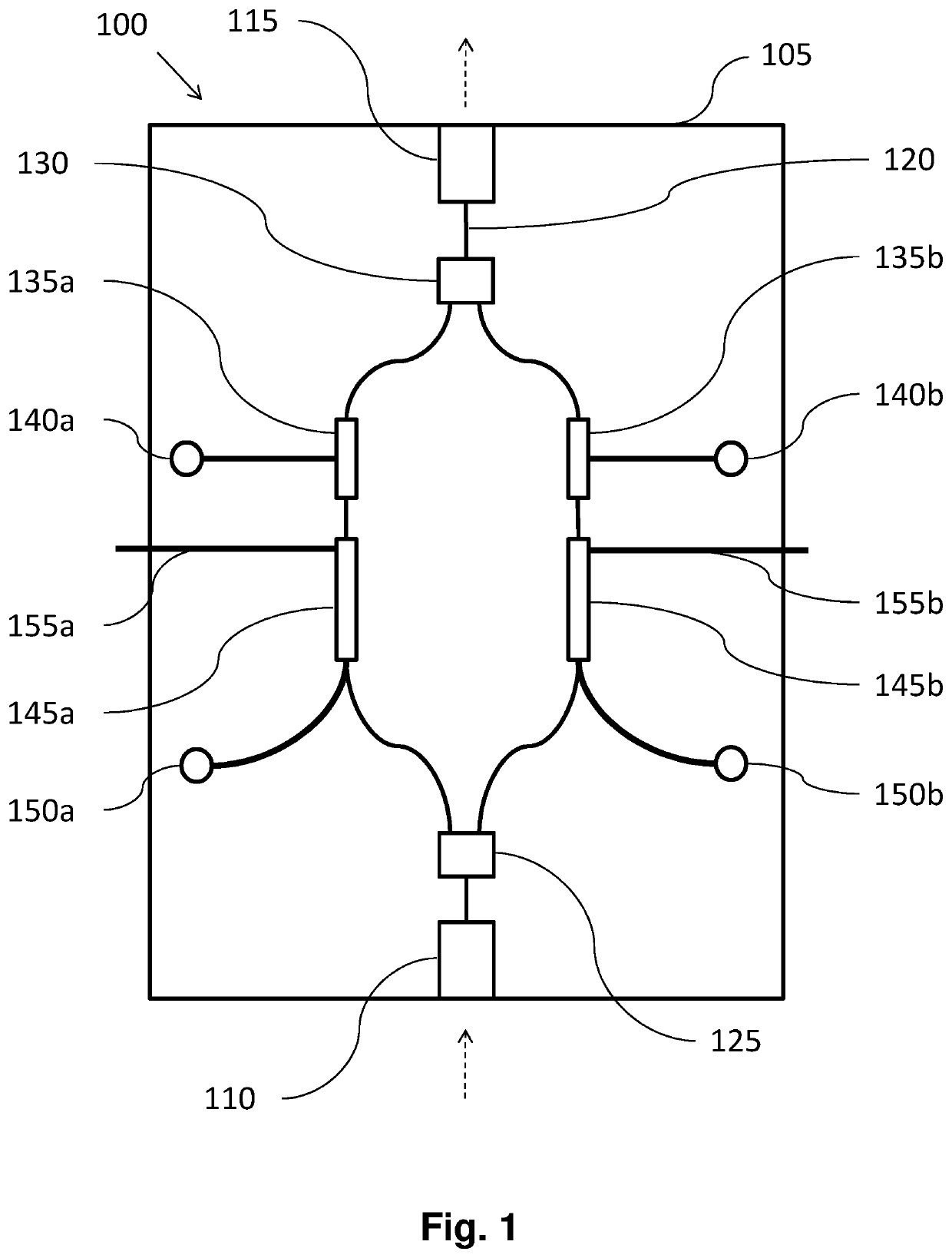
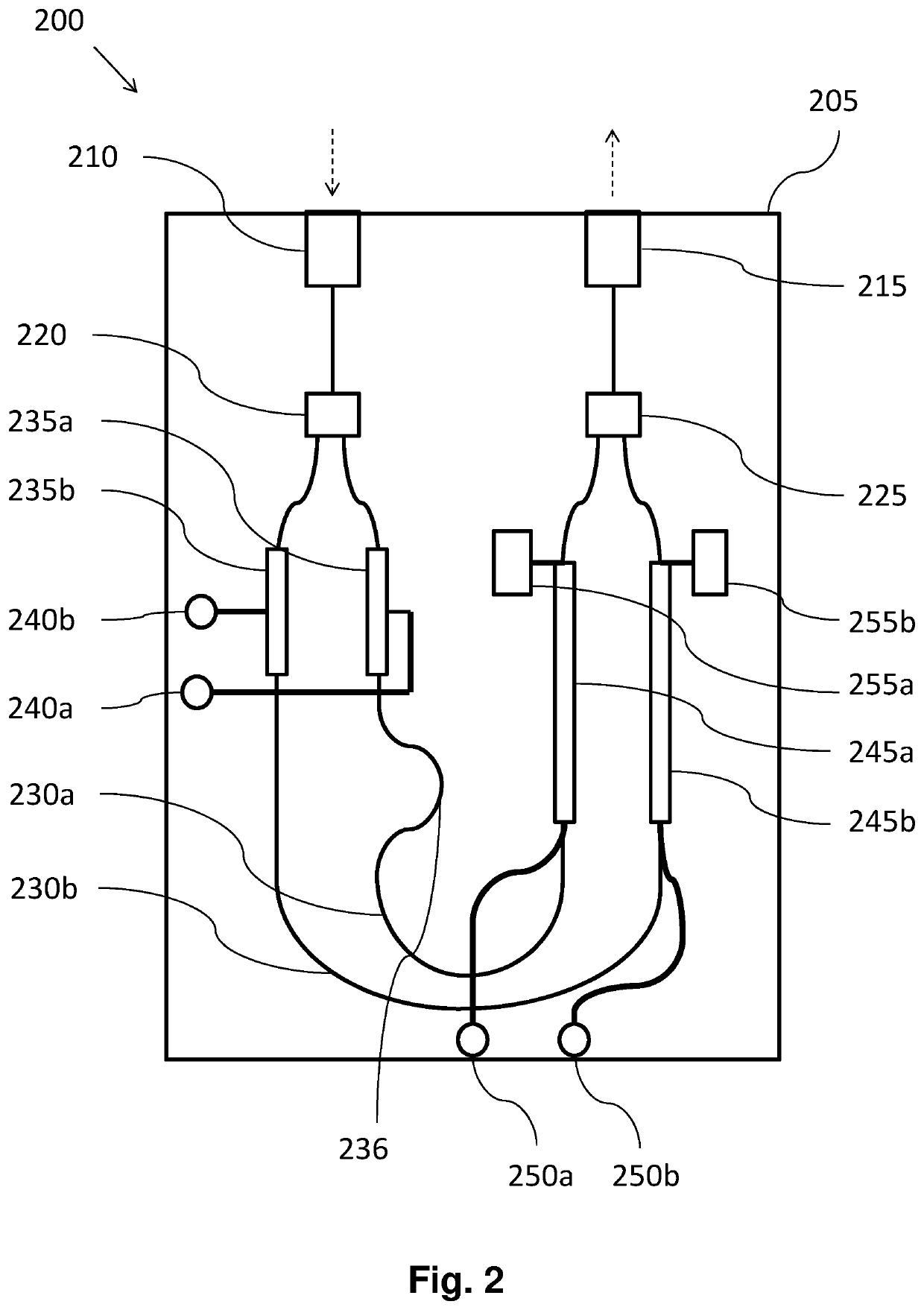
[0032]In causing the net 180° change in direction of the light while guiding said light from the input optical port to the output optical port, the waveguide may be configured to cause the light to propagate away from a central lengthwise axis of the device, thereby avoiding a crossover of the waveguide.

Problems solved by technology

Overall, the inventors have appreciated that installation of monolithically integrated optical modulator devices on multi-component optical modules is complex, expensive and time consuming.
Further, the current configuration of monolithically integrated optical modulator devices takes substantial design freedom away from the designers of multi-component optical modules, due to the spacing needed for such devices amongst other considerations.

Method used


Image

  • Optical modulation device
  • Optical modulation device
  • Optical modulation device

Examples


Embodiment Construction

[0049]Generally disclosed herein are optical modulation devices that are simple to install. The optical modulation devices disclosed herein allow for the construction of more compact and potentially complex multi-component optical modules.

[0050]The optical modulation devices disclosed herein are monolithically integrated and are generally configured to have their optical inputs and optical outputs disposed on a single front-facing edge, which will usually be a cleaved facet. By having an optical input disposed together with an optical output on a single facet of an optical modulation device, only that edge needs to be aligned when the device is installed on a multi-component module. In contrast, conventional optical modulation devices require both their front and rear facing edges to be aligned with respect to neighbouring components to ensure that its optical inputs and outputs can transmit and receive optical signals appropriately. Alignment of an additional facet adds an addition...


PUM

PropertyMeasurementUnit
widthaaaaaaaaaa
widthaaaaaaaaaa
widthaaaaaaaaaa

Abstract

The invention relates to optical modulation devices and, in particular, monolithically integrated optical modulation devices. Disclosed herein is a monolithically integrated optical modulation device (200) that comprises: an input optical port (210); an output optical port (215); and an optical waveguide for guiding light from the input optical port to the output optical port. A portion of the optical waveguide is split into at least two branches. The waveguide is configured to cause a net 180° change in direction of the light while guiding said light from the input optical port to the output optical port such that the input optical port and the output optical port are positioned on a first edge of the device. At least some of the net 180° change in direction is achieved within the branches of the waveguide.

Description

RELATED APPLICATIONS[0001]This application is a 35 U.S.C. 371 national stage filing of International Application No. PCT / GB2016 / 052677, filed on Aug. 30, 2016, which claims priority from United Kingdom Application No. GB1520472.0 filed on Nov. 20, 2015. The contents of the aforementioned applications are hereby incorporated by reference in their entireties.TECHNICAL FIELD[0002]The invention relates to optical modulation devices. The invention finds particular application in monolithically integrated optical modulation devices.BACKGROUND[0003]In this specification, the term “light” will be used in the sense that it is used in optical systems to mean not just visible light, but also electromagnetic radiation having a wavelength outside that of the visible range. Similarly, the terms “beam” and “beam of light” will be used to describe not just beams of visible light, but also electromagnetic radiation having a wavelength outside that of the visible range.[0004]In this specification, th...

Claims


Application Information

Patent Timeline
Patent Type & Authority Patents(United States)
IPC IPC(8): G02B6/125G02B6/12G02B6/02G02F1/225
CPCG02B6/125G02B6/02204G02B6/12007G02B2006/12142G02F1/225G02F1/2255
Inventor WARD, ANDREW JOHNWHITBREAD, NEIL DAVIDJONES, STEPHENCARTER, ANDREW CANNON
Owner LUMENTUM TECH UK LTD
Learn More