Touch sensor and touch panel

a touch sensor and touch panel technology, applied in the field of input devices, can solve the problems of inevitable increase in the thickness of the touch panel and increase the number of components, and achieve the effects of simple structure, reduced number of components of the touch panel, and high display quality

Active Publication Date: 2021-06-22
SEMICON ENERGY LAB CO LTD
View PDF22 Cites 0 Cited by
  • Summary
  • Abstract
  • Description
  • Claims
  • Application Information

AI Technical Summary

Benefits of technology

[0008]The display quality of the touch panel needs to be improved; for example, the contrast, luminance, and color reproducibility are necessary to increase.
[0010]An object of one embodiment of the present invention is to provide a thin touch panel. Another object is to provide a touch panel having a simple structure. Another object is to reduce the number of components of a touch panel. Another object is to provide a touch panel with high display quality. Another object is to provide an in-cell touch panel using an organic EL element. Another object is to provide a bendable touch panel. Another object is to provide a lightweight touch panel. Another object is to provide a touch panel with high detection sensitivity.
[0030]According to one embodiment of the present invention, a thin touch panel can be provided. Alternatively, a touch panel with a simple structure can be provided. Alternatively, the number of components of a touch panel can be reduced. Alternatively, a touch panel with high display quality can be provided. Alternatively, an in-cell touch panel using an organic EL element can be provided. Alternatively, a bendable touch panel can be provided. Alternatively, a lightweight touch panel can be provided. Alternatively, a touch panel with high detection sensitivity can be provided.

Problems solved by technology

However, this structure causes problems of an inevitable increase in the thickness of the touch panel, an increased number of components, and the like.

Method used


Image

  • Touch sensor and touch panel
  • Touch sensor and touch panel
  • Touch sensor and touch panel

Examples


embodiment 1

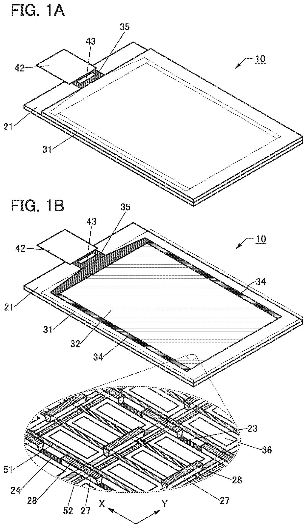
[0079]In this embodiment, a structure example of a touch panel of one embodiment of the present invention will be described. In particular, an example of using a capacitive touch sensor for the touch panel of one embodiment of the present invention will be described below.

[0080]Examples of the capacitive touch sensor include a surface capacitive touch sensor and a projected capacitive touch sensor. Examples of the projected capacitive touch sensor include a self-capacitive touch sensor and a mutual capacitive touch sensor. The mutual capacitive touch sensor is preferably used because multiple points can be sensed simultaneously.

[0081]The touch panel of one embodiment of the present invention includes a plurality of light-emitting elements arranged in a matrix. Each light-emitting element includes a first electrode (hereinafter referred to as a pixel electrode) serving as a pixel electrode, an EL layer, and a second electrode (hereinafter referred to as a common electrode) serving as...

modification example 1

[Modification Example 1 ]

[0162]In the above examples, the EL layer 37 is shared with a plurality of pixels. Alternatively, the EL layer 37 may be formed for every pixel emitting the same color, i.e., may be formed by a so-called side-by-side method.

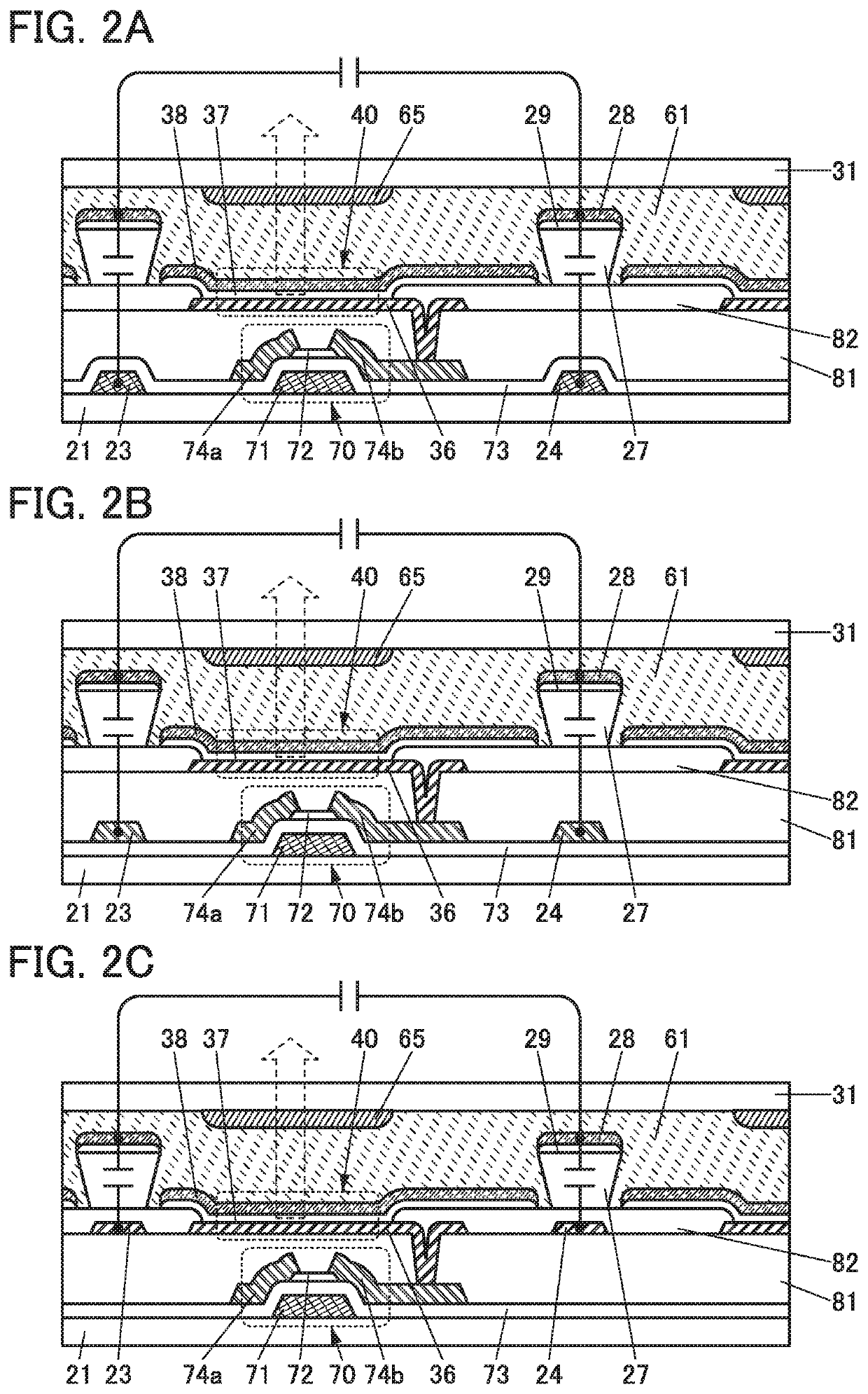
[0163]FIG. 8A shows an example in which the light-emitting element 40 is formed by a side-by-side method in the structure of FIG. 2A.

[0164]In FIG. 8A, the EL layer 37 is provided to cover an exposed portion of the pixel electrode 36. The EL layer 37 is formed in an island shape, and an end portion of the EL layer 37 is covered with the common electrode 38.

[0165]In this example, the EL layer 29 is not formed between the structure body 27 and the conductive layer 28.

[0166]Since the EL layer 37 emitting a different color light can be formed in each pixel, the coloring layer 65 does not need to be provided as illustrated in FIG. 8A, achieving a simplified structure of the substrate 31.

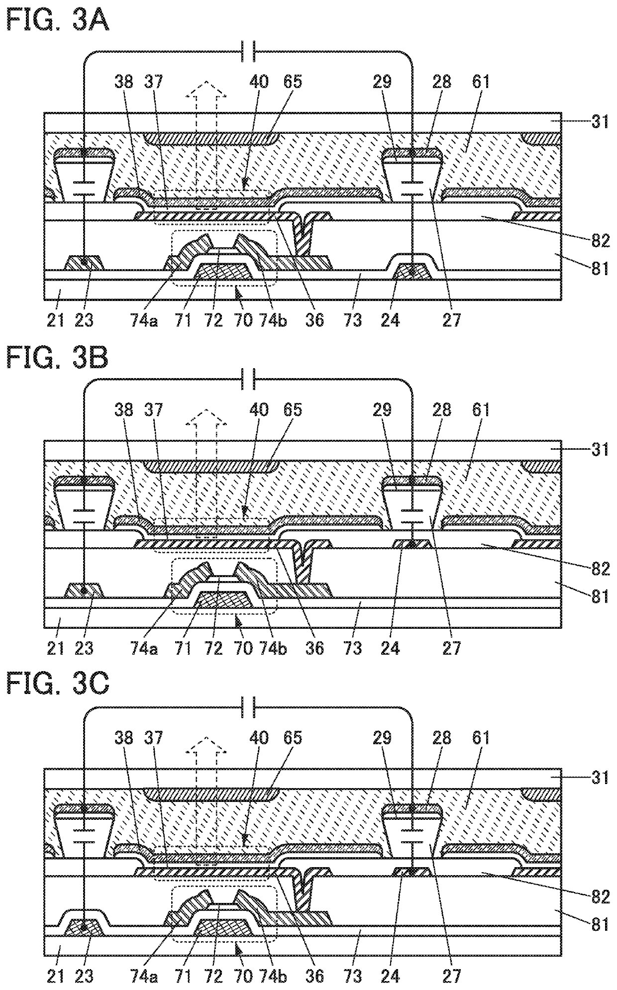
[0167]FIG. 8B shows an example in which the conductive lay...

example 1

[Arrangement Example 1 ]

[0212]FIGS. 13A to 13D show examples of the arrangement (layout) of the wiring 23, the wiring 24, the pixel electrode 36, the structure body 27, and the like. The examples illustrated in FIGS. 13A to 13D are preferably used in the case where, for example, the wirings 23 and 24 have a stripe shape in a portion overlapping with the display portion 32 as shown in Example 1 of Wiring Shape (FIGS. 11A and 11B and the like).

[0213]As illustrated in FIG. 13A, the wirings 23 extend in the X direction and the wirings 24 extend in the Y direction, and a grid-like shape is formed by these wirings. The pixel electrode 36 is provided inside one of the grids formed by the wirings 23 and 24.

[0214]A plurality of island-like structure bodies 27 are provided to overlap with the wirings 23 and 24. The structure bodies 27 are preferably arranged to overlap with either the wiring 23 or the wiring 24 so as not to cross the wirings 23 and 24.

[0215]FIG. 13A shows an example in which ...


PUM

PropertyMeasurementUnit
taper angleaaaaaaaaaa
sheet resistanceaaaaaaaaaa

Abstract

A thin touch panel is provided. A touch panel with a simple structure is provided. The number of components of a touch panel is reduced. Each of a pair of wirings of a touch sensor is positioned closer to a substrate supporting light-emitting elements than a common electrode is, and includes a portion positioned between two adjacent pixel electrodes in a plan view. Furthermore, an island-like structure body with an inverse tapered shape is provided over each of the pair of wirings. A conductive layer in an electrically floating state is provided over the structure body. Each conductive layer has a portion overlapping with one of the pair of wirings. Moreover, the conductive layer and the common electrode are formed using the same conductive film.

Description

BACKGROUND OF THE INVENTION1. Field of the Invention[0001]One embodiment of the present invention relates to an input device. One embodiment of the present invention relates to a display device. One embodiment of the present invention relates to an input / output device. One embodiment of the present invention relates to a touch panel.[0002]Note that one embodiment of the present invention is not limited to the above technical field. Examples of the technical field of one embodiment of the present invention disclosed in this specification include a semiconductor device, a display device, a light-emitting device, a power storage device, a memory device, an electronic device, a lighting device, an input device, an input / output device, a driving method thereof, and a manufacturing method thereof.[0003]Note that in this specification and the like, a semiconductor device refers to any device that can function by utilizing semiconductor characteristics. Not only a semiconductor element such...

Claims


Application Information

Patent Timeline
Patent Type & Authority Patents(United States)
IPC IPC(8): G06F3/041H01L27/32G06F3/044
CPCH01L27/3246G06F3/0412G06F3/0443G06F3/0446H01L27/323H01L27/3276G06F2203/04102G06F2203/04103G06F2203/04112H01L2251/5338G06F3/044G06F2203/04104G06F2203/04111H10K59/40H10K59/122H10K59/131H10K2102/311G06F3/0445
Inventor YOSHIZUMI, KENSUKESHISHIDO, HIDEAKIWATANABE, KAZUNORI
Owner SEMICON ENERGY LAB CO LTD
Why Eureka
Try Eureka