
Dike for semiconductor/LCD manufacturing and processing equipment

a technology for processing equipment and semiconductors, applied in water installations, applications, other domestic objects, etc., can solve the problems of increasing manufacturing costs, contaminating the workplace, and taking a long time to form the dike, and achieve the effect of easy and quick collection of contaminants and easy removal

Active Publication Date: 2021-07-13
KIM JUNG SOO
View PDF10 Cites 0 Cited by
  • Summary
  • Abstract
  • Description
  • Claims
  • Application Information

AI Technical Summary

Benefits of technology

[0012]The present invention has been made in view of the above problems, and it is an object of the present invention to provide a dike for semiconductor-manufacturing equipment, which is formed by installing a fence in a predetermined area on a floor of a building on which semiconductor-manufacturing equipment is installed and by injecting molten epoxy into the space within the fence and solidifying the epoxy, and which is capable of increasing the rigidity of the fence, facilitating installation of the fence, preventing the molten epoxy injected in the dike from leaking outside through the corners of the fence, facilitating collection of contaminants accumulated in the dike, and facilitating removal of the epoxy adhered to the floor of the building when dismantling the equipment equipped with the dike.
[0017]The epoxy injected in the dike may be formed as a horizontal epoxy having a uniform thickness on the floor inside the fence. Alternatively, an inclined epoxy block, having an inclined surface inclined at a predetermined angle, may be mounted on a predetermined portion of the top surface of the horizontal epoxy in order to form a contaminant discharge path at the lower end of the inclined surface of the inclined epoxy block, thereby enabling easy and quick collection of contaminants accumulated in the dike.
[0018]A TEFLON sheet, having an adhesive attached to the bottom surface thereof, may be adhered to the floor inside the fence, and molten epoxy may be applied to the top surface of the TEFLON sheet and solidified, thereby making it possible to easily remove the epoxy adhered to the floor inside the fence when moving or dismantling semiconductor-manufacturing equipment.

Problems solved by technology

There is a problem in that liquid scatters or leaks outside the semiconductor-manufacturing equipment onto the floor during operation, thus contaminating the workplace.
Therefore, it takes a long time to form the dike, and the manufacturing costs thereof increase.
Since the portion of the fence of the dike in which the epoxy is not fully injected has insufficient strength, it is easily broken or damaged by external forces, for example, when stepped on by a worker or touched by a cleaning tool, which leads to a problem of frequent reconstruction of the dike.
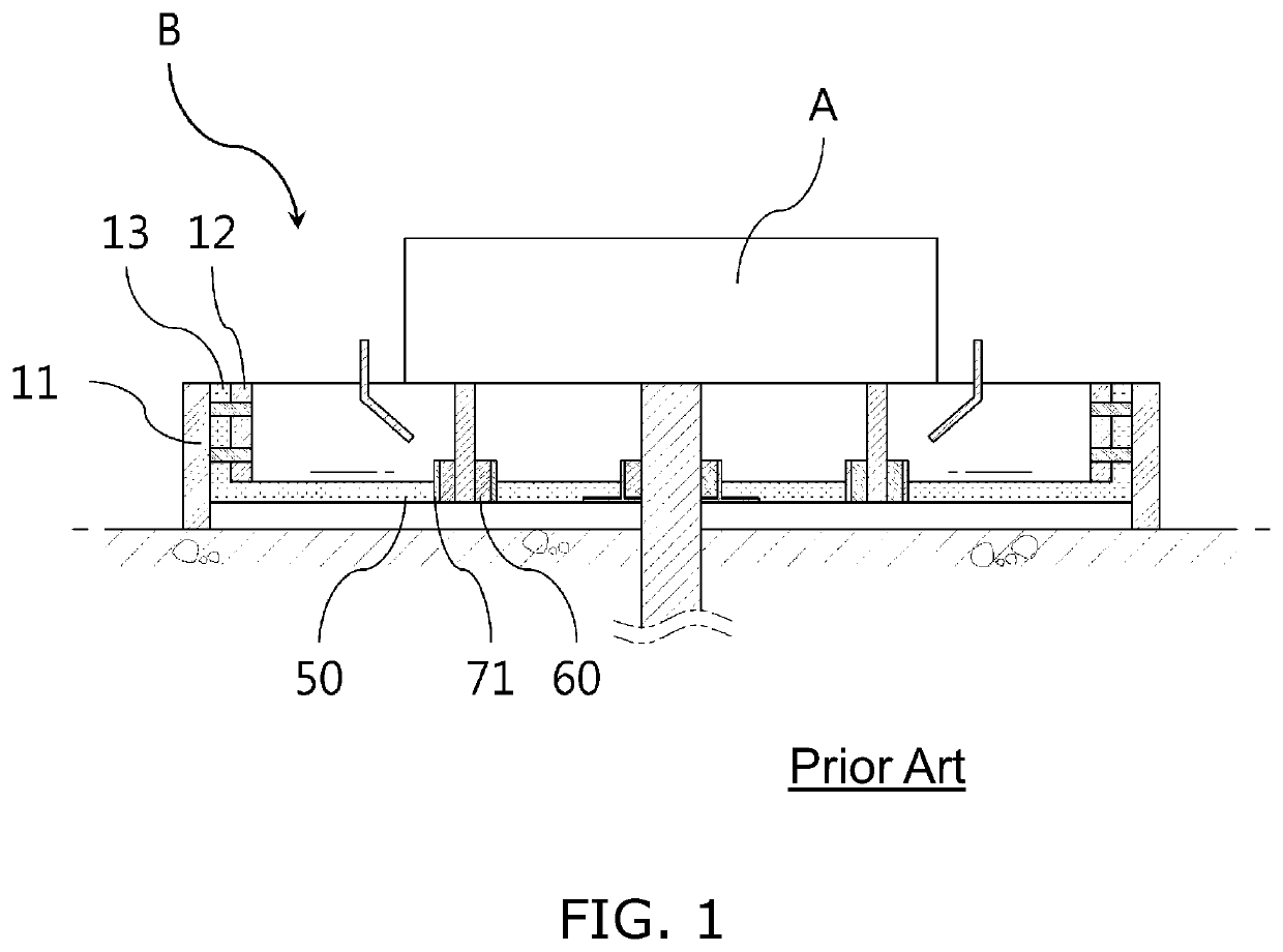
In addition, in the above conventional patent technology, since the fence is formed to include corners at which the outer walls 11, to which the inner walls 12 are coupled, join each other perpendicularly, there occurs a problem in that the molten epoxy injected into dike leaks outside through gaps in the corners of the fence.
In addition, in the above conventional patent technology, in which the fence is formed to include corners at which the outer walls 11, to which the inner walls 12 are coupled, join each other perpendicularly, since it is difficult to connect the ends of neighboring outer walls to each other perpendicularly, separate fixtures are used or an installation area needs to be marked in advance on the floor when the dike is constructed, which leads to a problem of complicated and time-consuming installation.
In addition, in the above conventional patent technology, since an epoxy is injected in the dike and solidified in the form of a horizontal plane having a uniform thickness, liquid contaminants generated in the semiconductor-manufacturing equipment are stored to a uniform height in the entire area of the dike, which leads to a problem of slow and difficult collection of the contaminants.
However, the molten epoxy permeates the pulp paper and adheres to the floor, which leads to a problem of difficulty of removal of the epoxy from the floor when moving or dismantling the equipment.

Method used


Image

  • Dike for semiconductor/LCD manufacturing and processing equipment
  • Dike for semiconductor/LCD manufacturing and processing equipment
  • Dike for semiconductor/LCD manufacturing and processing equipment

Examples


Embodiment Construction

[0028]Embodiments described in the specification and the configuration of elements illustrated in the drawings are merely considered to be preferred embodiments and do not represent all the technical ideas of the present disclosure, and thus it should be understood that various equivalents and modifications may exist at the time of filing this application.

[0029]Hereinafter, a dike for semiconductor-manufacturing equipment according to the present invention will be described in detail with reference to the accompanying drawings. In the description of the present invention, the same terms and reference numerals are used to designate components that perform the same functions as those in the conventional art.

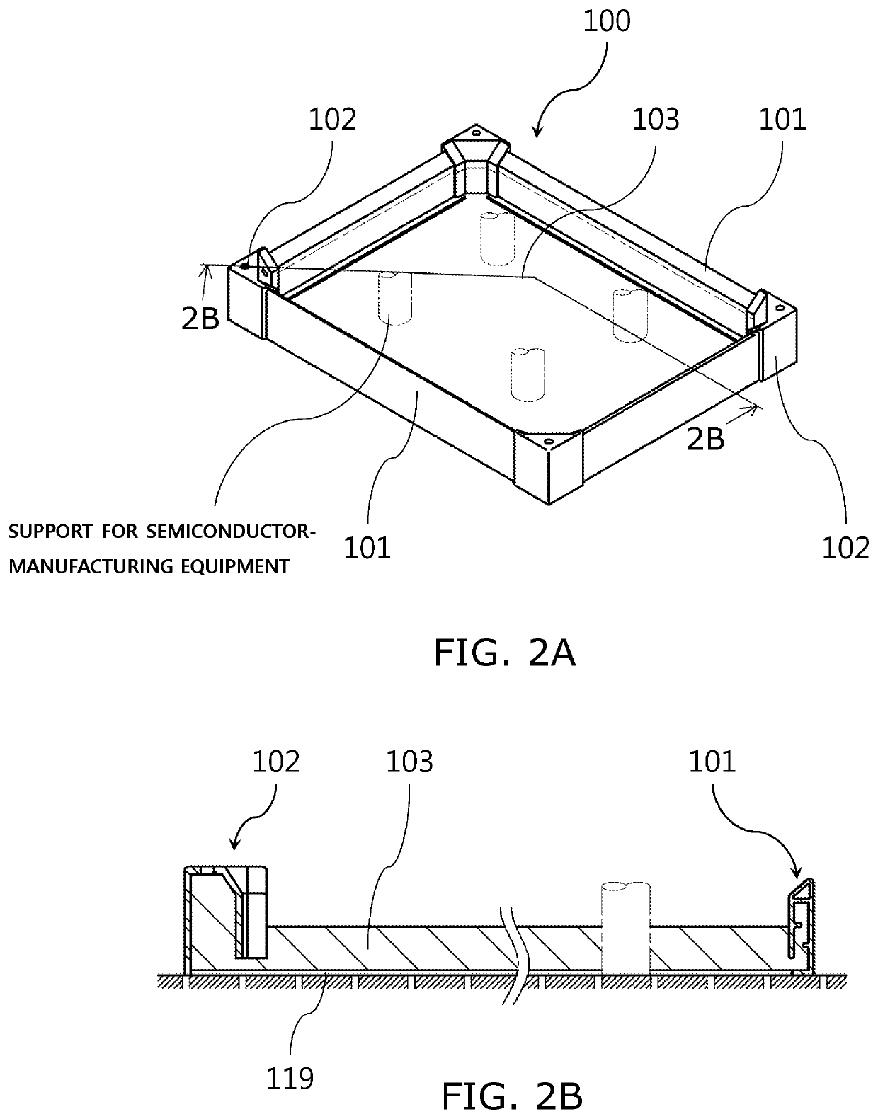
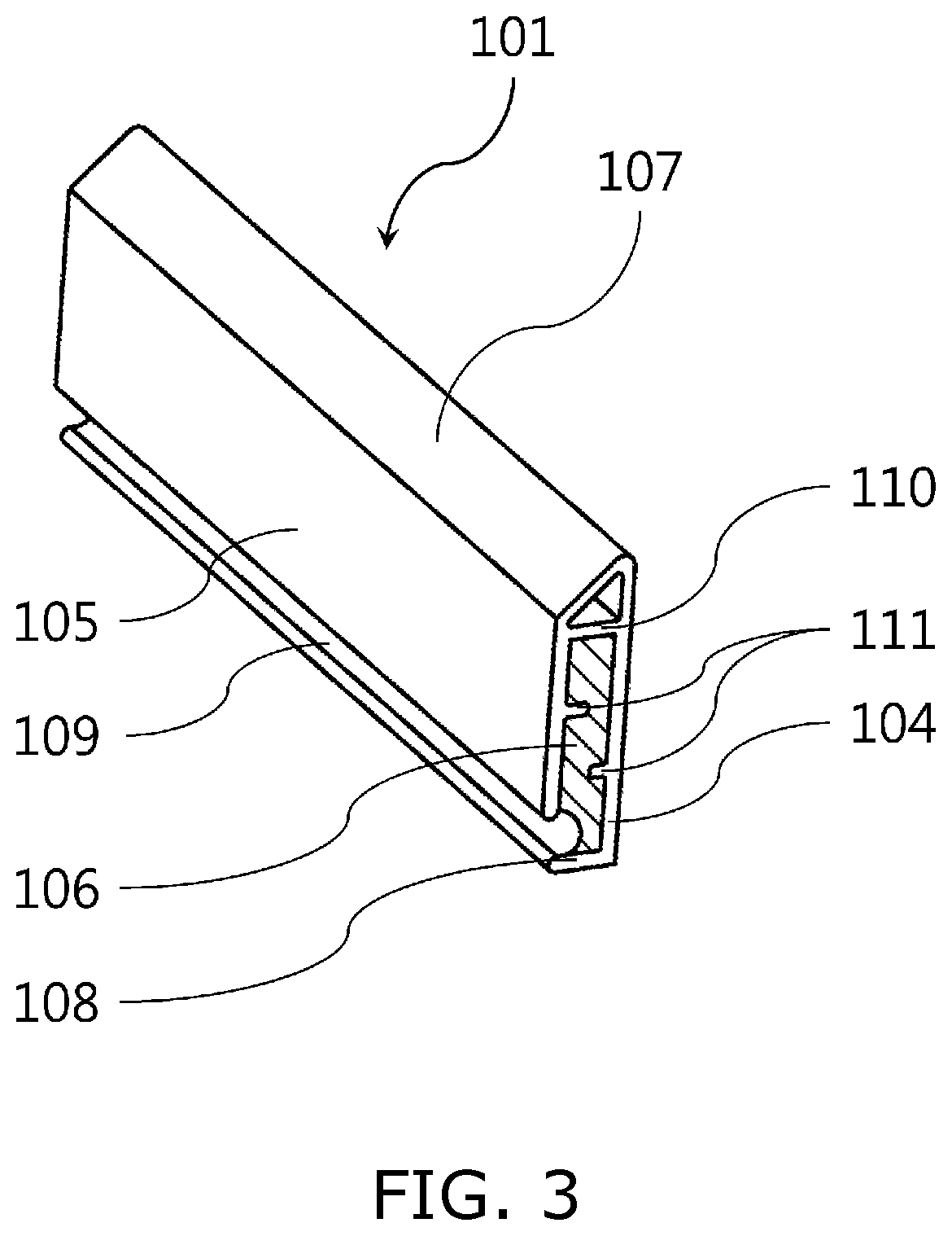
[0030]As shown in FIGS. 2A and 2B, the present invention relates to a dike 100 for collecting and processing liquid that leaks or scatters from semiconductor-manufacturing equipment installed on a porous floor of a building, in which a plurality of straight blocks 101 and a plurali...


PUM

PropertyMeasurementUnit
heightaaaaaaaaaa
widthaaaaaaaaaa
included angleaaaaaaaaaa

Abstract

Disclosed is a dike for semiconductor / LCD manufacturing and processing equipment, in which a plurality of straight blocks and a plurality of corner blocks, having a predetermined height, are engaged to form a polygonal-shaped fence having a predetermined area, and molten epoxy is injected to a predetermined height in the space within the fence and solidified.

Description

BACKGROUND OF THE INVENTIONField of the Invention[0001]The present invention relates to a dike for semiconductor / LCD manufacturing and processing equipment (hereinafter, referred to as “semiconductor-manufacturing equipment”), and more particularly to technology for forming a dike for receiving and collecting contaminants that scatter or leak to the surrounding floor from semiconductor-manufacturing equipment that uses liquid such as water or chemicals.Description of the Related Art[0002]In general, semiconductor-manufacturing equipment includes equipment for performing processes such as chemical vapor deposition, etching, or cleaning, and this equipment is installed on a porous floor of a building and uses liquid such as water, solvents, and chemicals. There is a problem in that liquid scatters or leaks outside the semiconductor-manufacturing equipment onto the floor during operation, thus contaminating the workplace.[0003]In order to solve this problem, a dike for collecting liqui...

Claims


Application Information

Patent Timeline
Patent Type & Authority Patents(United States)
IPC IPC(8): H01L21/67H01L21/02B29C45/00B29C45/14B29C45/26B29K63/00B29K627/18B29L31/10
CPCH01L21/67017B29C45/0001B29C45/14336B29C45/2602H01L21/02041H01L21/6715B29K2063/00B29K2627/18B29L2031/10E03F5/10H01L21/67259
Inventor KIM, JUNG SOO
Owner KIM JUNG SOO
Learn More