Sensors with gradient nanostructures and associated method of use

a nanostructure, nano-structure technology, applied in measurement devices, instruments, scientific instruments, etc., can solve the problem that colorimetric sensors cannot provide highly accurate, etc., and achieve the effect of high accuracy, time-saving and cost-effectiv

Active Publication Date: 2021-07-20
VERSITECH LTD
View PDF29 Cites 0 Cited by
  • Summary
  • Abstract
  • Description
  • Claims
  • Application Information

AI Technical Summary

Benefits of technology

[0008]A machine learning model has been developed to recognize the image patterns displayed by the sensor through an image recognition method, and with sufficient training data, the model can be used to extract the environment property with high accuracy based on the sensor image.
[0009]The fabrication method of the present invention is based on interference lithography and nanoimprint, which is more time-effective and cost-efficient than arbitrary lithography techniques like e-beam lithography or ion milling.
[0010]The present invention operates for a wide range of environmental characteristics because the sensing area contains spatially varying structures, so a broader range of environmental properties can be sensed more effectively at specific structures.

Problems solved by technology

Conventionally, sensing methods applied on these sensors are typically based on reflection or transmission spectrum analysis, which are expensive and time consuming Another type of sensing method is based on colorimetry.
However, these colorimetric sensors cannot provide highly accurate results because they are limited by the color distinguishing ability of human eyes.

Method used


Image

  • Sensors with gradient nanostructures and associated method of use
  • Sensors with gradient nanostructures and associated method of use
  • Sensors with gradient nanostructures and associated method of use

Examples


example 1

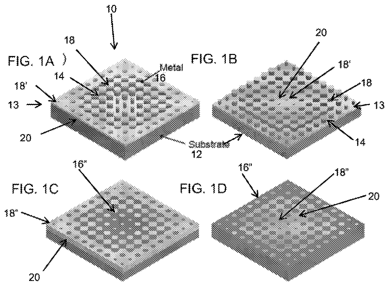
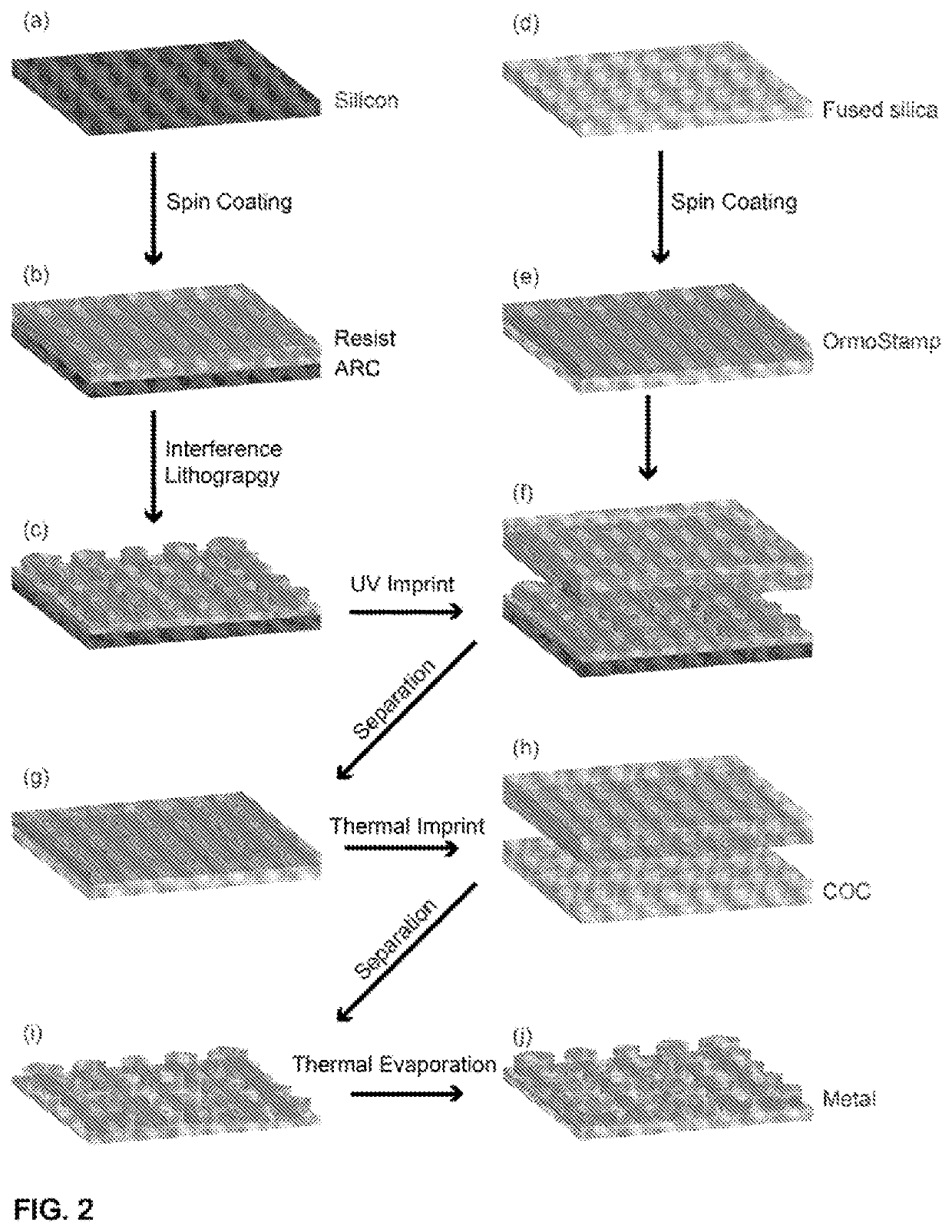
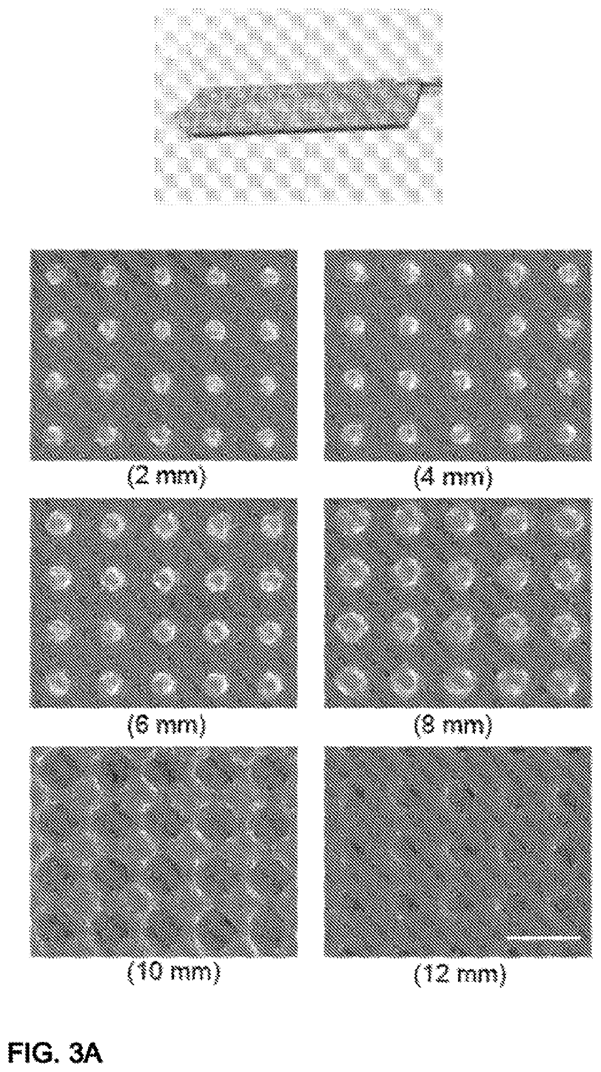
[0031]An embodiment of the present invention was fabricated as seen in FIGS. 3A-B, In the sensor embodiment of FIGS. 3A-B, a sensor with pillar-hole structures covered by gold disks and nano-hole plane was fabricated using the above stated fabrication procedure with interference lithography being used to pattern the resist.

[0032]FIG. 3A shows the gradient color rings displayed by gradient nanostructures on a silicon substrate. SEM characterizations show the nano pillars and holes at different radial distances in the resist. The nanostructures have a period of 370 nm. Then the gradient pattern was transferred to a fused silica wafer by UV imprint lithography to create a thermal imprint template. Then, a thermoplastic film such as a cyclic olefin copolymer (“COC”) film was placed on the fused silica template with a gradient pattern, heated, pressed and separated. Finally, an 80 nm gold layer was deposited on the COC film by thermal evaporation. As a result, a sensor with pillar-hole s...

example 2

[0034]A gradient-pattern plasmonic sensor according to an embodiment of the present invention can be used in a spectrometer-free way. A schematic of an approach for using the gradient-pattern plasmonic sensor according to an embodiment of the present invention can be seen in FIG. 4. The setup used for liquid refractive index measurement using a sensor 10 with pillar-hole structures covered by gold disks and nano-hole planes according to an embodiment of the present invention includes: (i) a white illumination light source 40, illuminating the sensor 10 from the back side; (ii) the sensor is covered with refractive index liquid 42; and (iii) a camera 44 taking pictures from the front side. The camera may be a cellphone camera or a CMOS or a CCD camera. The liquid 42 can be any one of a number of functional materials, e.g., palladium, hydrogel, an antibody, protein, gas molecules, ions in water, antigen and DNA.

[0035]In one arrangement an iPhone was used with a white background screen...


PUM

PropertyMeasurementUnit
thicknessaaaaaaaaaa
single wavelengthaaaaaaaaaa
heightaaaaaaaaaa

Abstract

A plasmonic sensor with gradient nanostructures and a method of use thereof is provided. The gradient of shapes will induce different spectral responses at different region of the sensor and show different colors. When there is a change in the environment properties of a substance, such as refractive index, gas concentration or ion density changes, the sensor displays different images, e.g., redial intensity displays and radial color displays. An image recognition based method can be used to extract the environment property with high accuracy according to the sensor image.

Description

CROSS-REFERENCE TO RELATED PATENT APPLICATIONS[0001]This application is a U.S. National Phase Application under 35 U.S.C. § 371 of International Patent Application No. PCT / CN2018 / 089512, filed Jun. 1, 2018 and claims the benefit of priority under 35 U.S.C. Section 119(e) of U.S. Application Ser. No. 62 / 513,631, filed Jun. 1, 2017; which are incorporated herein by reference in their entireties. The International Application was published in English on Dec. 6, 2018 as International Publication No. WO 2018 / 219344 A1.FIELD OF THE INVENTION[0002]The present invention relates generally to nanostructured devices and, more particularly, to the fabrication and use of optical devices with gradient nanostructures for sensing biological and environmental parameters.BACKGROUND OF THE INVENTION[0003]Devices with nanostructures are widely used in biomedical sensing and environmental monitoring. The nanostructures are well designed and carefully fabricated to enhance the signal intensity. For fabri...

Claims


Application Information

Patent Timeline
Patent Type & Authority Patents(United States)
IPC IPC(8): G01N21/552B82Y15/00
CPCG01N21/554B82Y15/00
Inventor LI, WENDIZHU, ZHOUYANGLI, SHIJIE
Owner VERSITECH LTD
Why Eureka
Try Eureka