

Photoelectric converter and process for producing the same and solid state imaging device
- Summary
- Abstract
- Description
- Claims
- Application Information
AI Technical Summary
Benefits of technology
Problems solved by technology
Method used
Image

Examples
first embodiment
(Plane Pattern Configuration)
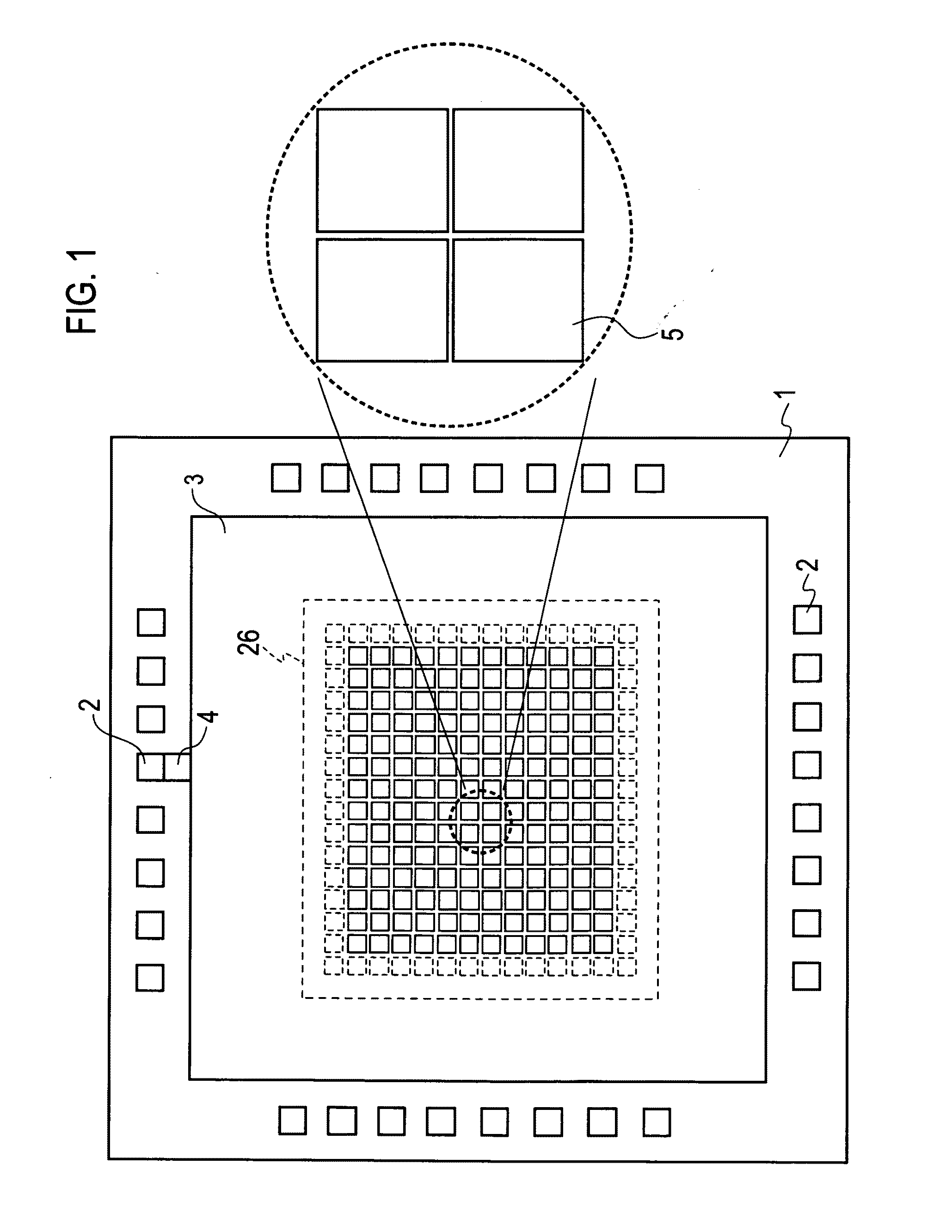
FIG. 1 shows an overall schematic plane pattern configuration of a solid state imaging device formed by two-dimensionally arranging photoelectric converters according to a first embodiment of the present invention. As shown in FIG. 1, the solid state imaging device includes: a package substrate 1; multiple bonding pads 2 disposed in a peripheral part on the package substrate 1; and an aluminum electrode layer 3 which is connected to one of the bonding pads 2 by a bonding pad connector 4, and is connected along the peripheral part of the solid state imaging device to a transparent electrode layer 26 disposed on pixels 5 of the solid state imaging device. Specifically, the aluminum electrode layer 3 covers an edge region of the transparent electrode layer 26, and is connected to one of the bonding pads 2 by the bonding pad connector 4. Moreover, the pixels 5 are arranged in a matrix pattern in the example shown in FIG. 1.
(Photoelectric Converter)
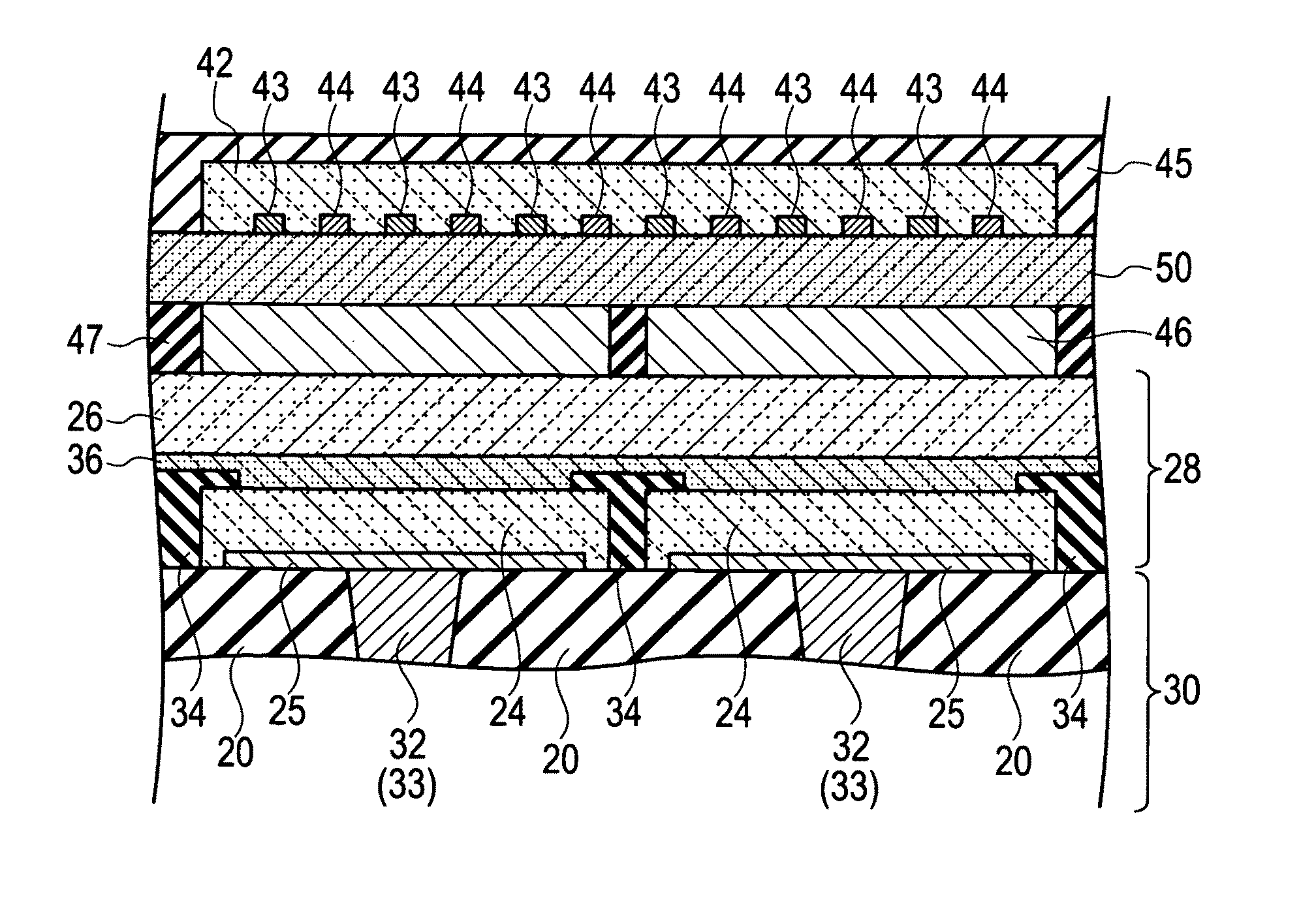
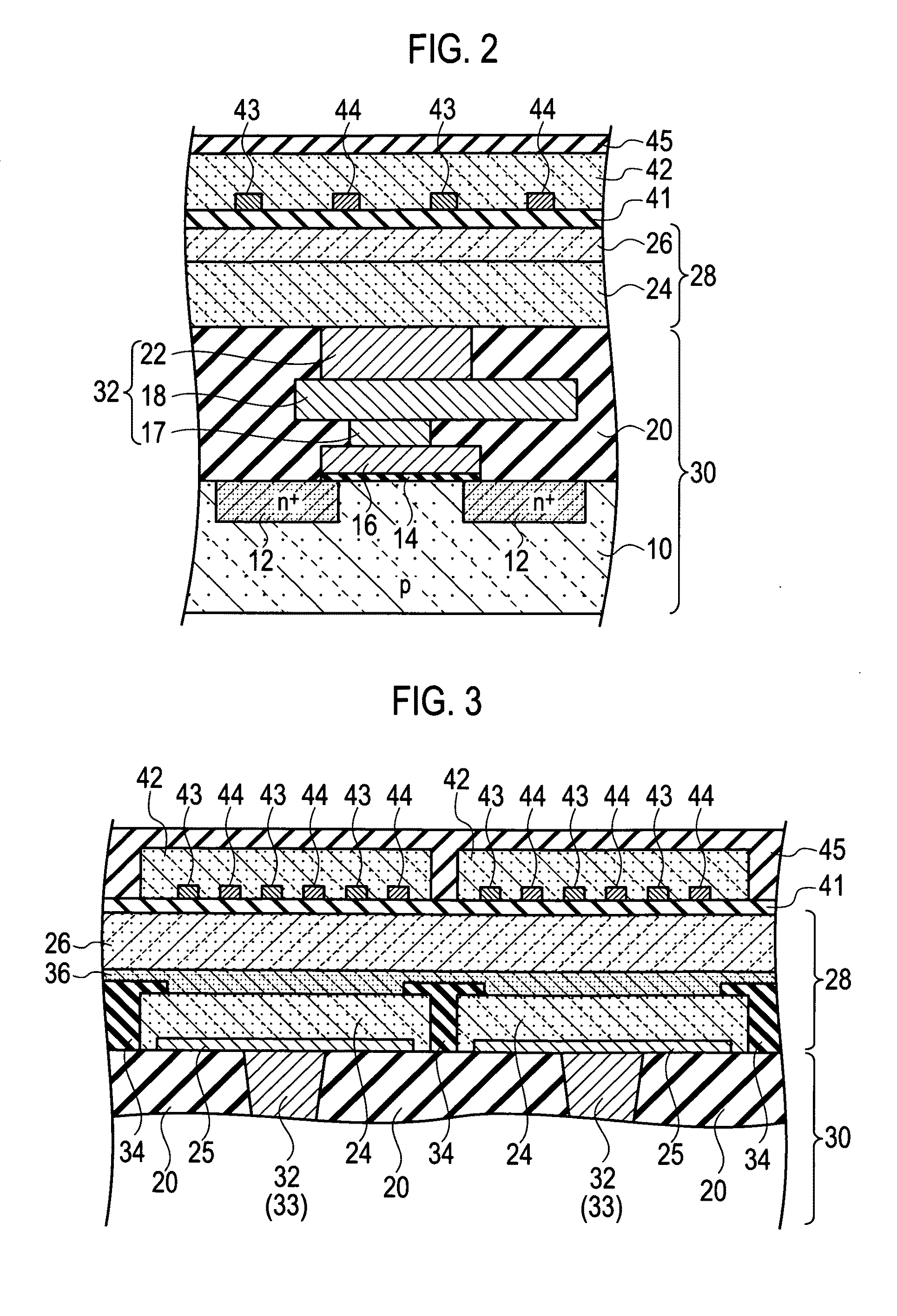
FIG. 2 sho...
second embodiment
(Plane Pattern Configuration)
A whole schematic plane pattern configuration of a solid state imaging device configured by two-dimensionally arranging photoelectric converters according to a second embodiment of the present invention is the same as that shown in FIG. 1. Therefore, description thereof is omitted.
(Photoelectric Converter)
FIG. 32 shows a schematic cross-sectional structure of the photoelectric converter according to the second embodiment. As shown in FIG. 32, the photoelectric converter includes: a circuit portion 30 formed on a substrate; and a photoelectric conversion unit 28 disposed on the circuit portion 30. Note that FIG. 32 omits illustration of a lower electrode layer 25 and a buffer layer 36.
The photoelectric converter shown in FIG. 32 includes: the circuit portion 30 formed on a semiconductor substrate 10; the lower electrode layer 25 disposed on the circuit portion30; a compound semiconductor thin film 24 of chalcopyrite structure disposed on the lower electro...
PUM
 Abstract
Description
Claims
Application Information