Optical transceiver module and optical cable module

a technology of optical transceivers and optical cables, applied in the field of optical fiber communication technology, can solve the problems of optical modules such as optical transceivers that are required to be further downsized, electrical i/o signal rates are limited, and the conventional electrical i/o (input/output) signaling cannot keep up with the demand for performance increases, etc., and achieves the effect of simple manufacturing structur

Active Publication Date: 2021-08-31
YU SHENG PHOTOELECTRIC CO LTD
View PDF1 Cites 3 Cited by
  • Summary
  • Abstract
  • Description
  • Claims
  • Application Information

AI Technical Summary

Benefits of technology

[0007]In varied embodiments of the present invention, the substrate can comprise at least one convex portion and at least one recess portion, and the at least one convex portion protrudes to the substrate, and the at least one recess portion is positioned to at least one side of the convex portion. Circuits or at least one IC chip can be disposed on a surface of the at least one convex portion of the substrate, so as to increase the setting area for the circuits.
[0035]The present invention provides an optical transceiver module effectively utilizing the internal space thereof for a compact design. Moreover, the optical transceiver module of the invention can have a simple structure for manufacturing.

Problems solved by technology

However, conventional electrical I / O (input / output) signaling is not expected to keep pace with the demand for performance increases, especially for a higher performance computing expectations.
Therefore, electrical I / O signal rates are limited by the electrical characteristics of the electrical connectors.
However, in recent years, the optical modules such as optical transceiver are required to be further down-sized.

Method used


Image

  • Optical transceiver module and optical cable module
  • Optical transceiver module and optical cable module
  • Optical transceiver module and optical cable module

Examples


Embodiment Construction

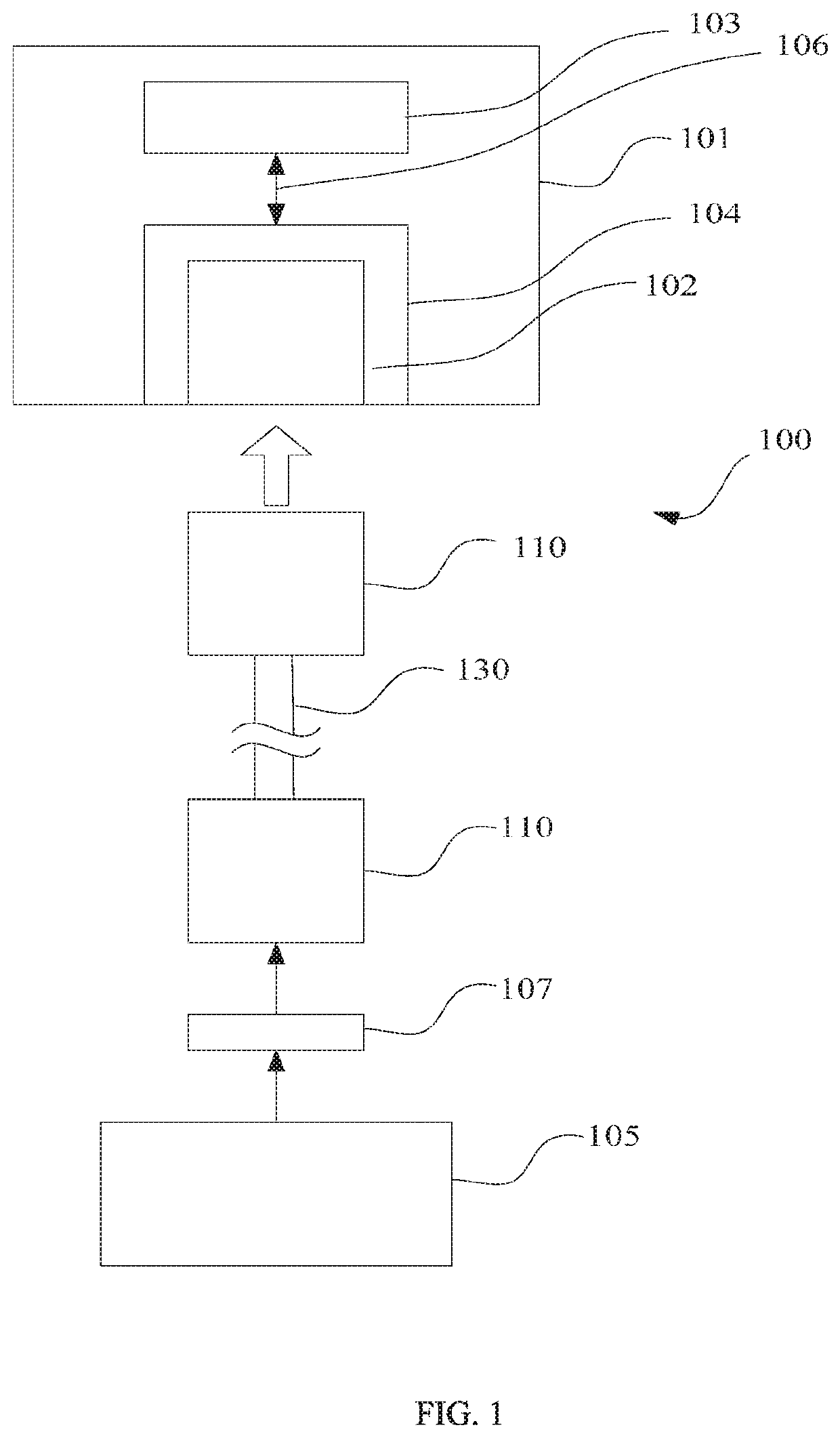
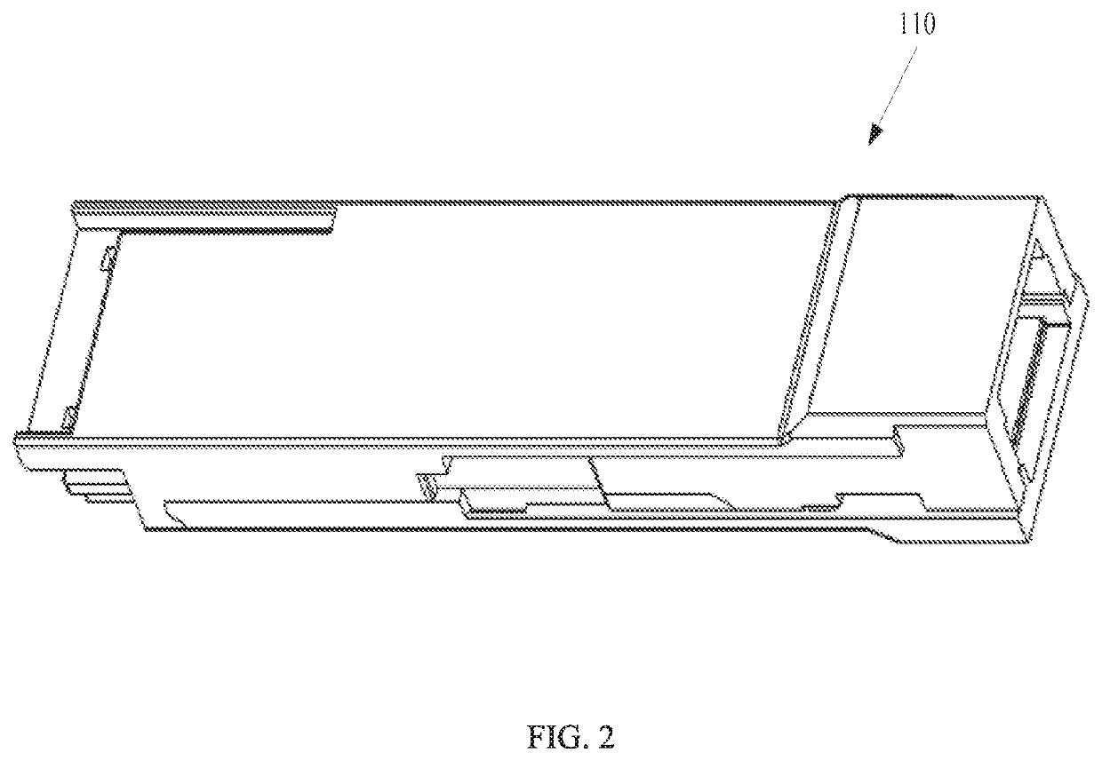
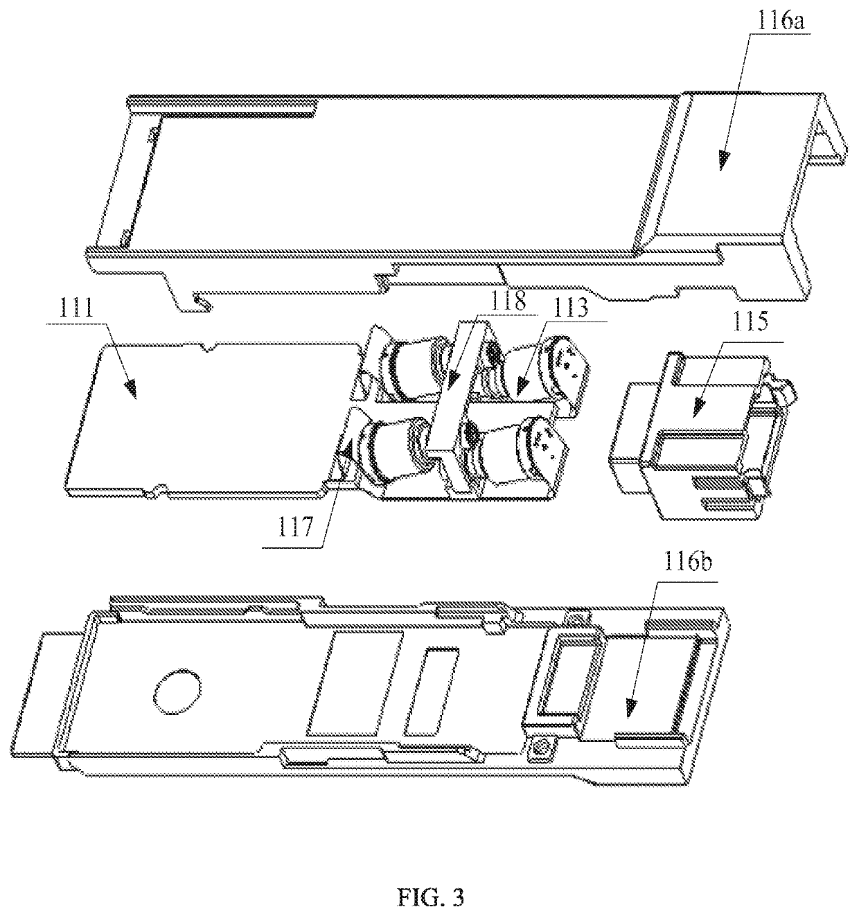
[0056]The following embodiments are referring to the accompanying drawings for exemplifying specific implementable embodiments of the present invention. Furthermore, directional terms described by the present invention, such as upper, lower, front, back, left, right, inner, outer, side, etc., are only directions by referring to the accompanying drawings, and thus the used directional terms are used to describe and understand the present invention, but the present invention is not limited thereto.

[0057]The drawings and description are to be regarded as illustrative in nature and not restrictive. Like reference numerals designate like elements throughout the specification. In addition, the size and thickness of each component shown in the drawings allow ease of understanding and ease of description, but the present invention is not limited thereto.

[0058]In the drawings, the thickness of layers, films, panels, regions, etc., are exaggerated for clarity. In the drawings, for understandi...


PUM

PropertyMeasurementUnit
tilt angleaaaaaaaaaa
angleaaaaaaaaaa
tilt angleaaaaaaaaaa

Abstract

The present invention is to provide an optical transceiver module comprising a housing, a substrate, an optical receiving device and a plurality of optical transmitting devices. The substrate is disposed in the housing. The optical receiving device is disposed on the substrate. The plurality of optical transmitting devices are connected to the substrate, and there is a tilt angle between the optical transmitting devices and the substrate.

Description

FIELD OF THE INVENTION[0001]The present invention relates to an optical fiber communication technology field, and in particularly, to an optical transceiver module and an optical fiber cable module using the same.BACKGROUND OF THE INVENTION[0002]In the optical fiber communication technology, it is necessary to convert electrical signals into optical signals through an optical transceiver module (such as a laser device), and then to couple the optical signals into an optical fiber for transmitting. At present, the demand for computing devices continues to rise, even as the demand for computing devices to achieve higher performance also rises. However, conventional electrical I / O (input / output) signaling is not expected to keep pace with the demand for performance increases, especially for a higher performance computing expectations. Currently, I / O signals are sent electrically to and from the processor through the board and out to peripheral devices. Electrical signals must pass thro...

Claims


Application Information

Patent Timeline
Patent Type & Authority Patents(United States)
IPC IPC(8): G02B6/42H04B10/40
CPCG02B6/4246H04B10/40G02B6/4239G02B6/4245G02B6/4251G02B6/4271G02B6/4277G02B6/4281G02B6/4284
Inventor CHANG, CHUN-YANGHUANG, YUN-CHENGLI, WEN-HSIENLU, CHENG-HUNGCHEN, MING-JUWU, CHANG-CHERNG
Owner YU SHENG PHOTOELECTRIC CO LTD
Why Eureka
Try Eureka