Display

a technology of display and ink, applied in the field of display, can solve the problems of color mixing problem, inability to print, ink bridging of ink in adjacent pixels, and inability to print, etc., and achieve the effect of increasing the success rate of printing

Active Publication Date: 2021-11-02
SHENZHEN CHINA STAR OPTOELECTRONICS SEMICON DISPLAY TECH CO LTD
View PDF12 Cites 0 Cited by
  • Summary
  • Abstract
  • Description
  • Claims
  • Application Information

AI Technical Summary

Benefits of technology

[0004]In view of the above, the present invention provides a display including a novel pixel design, combining partial pixels in a long axis or a short axis direction to form a strip-shaped opening in a pixel definition layer, thereby enlarging a printing area to solve the problems of the current harsh demands for the ink drop accuracy and the drop control system, and increase the success rate of printing.
[0018]The invention provides a display including a novel pixel design, combining partial pixels in a long axis or a short axis direction to form a strip-shaped opening in a pixel definition layer, thereby enlarging a printing area to solve the problems of the current harsh demands for the ink drop accuracy and the drop control system, and increase the success rate of printing.

Problems solved by technology

It does not allow misprinting, missing printing, and ink bridging of the ink in adjacent pixels.
Otherwise, it will lead to uneven film thickness, and a color mixing problem will occur due to the ink bridging during printing a light-emitting layer.
Even a one-millionth printing abnormal probability will cause a number of defective pixels in the entire panel to exceed a normal specification tolerance (≤3), so the traditional panel SBS pixel design concept is difficult to meet the high-resolution panel preparation requirements.

Method used


Image

  • Display
  • Display
  • Display

Examples


Embodiment Construction

[0024]In order to make the above description of the present invention more comprehensible, the preferred embodiments are described below in detail with reference to the accompanying drawings.

[0025]The following description of the various embodiments is provided to illustrate the specific embodiments of the invention. Directional terms mentioned in the present invention, such as “vertical”, “horizontal”, “upper”, “bottom”, “pre”, “post”, “left”, “right”, “inside”, “outside”, “side”, etc., only refer to the direction of the additional drawing. Therefore, the directional terminology used is for the purpose of illustration and understanding of the invention. In the figures, structurally similar elements are denoted by the same reference numerals.

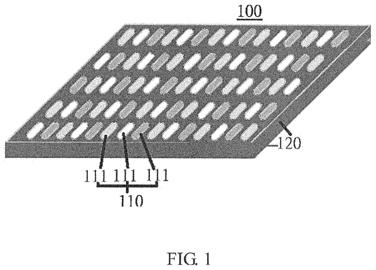
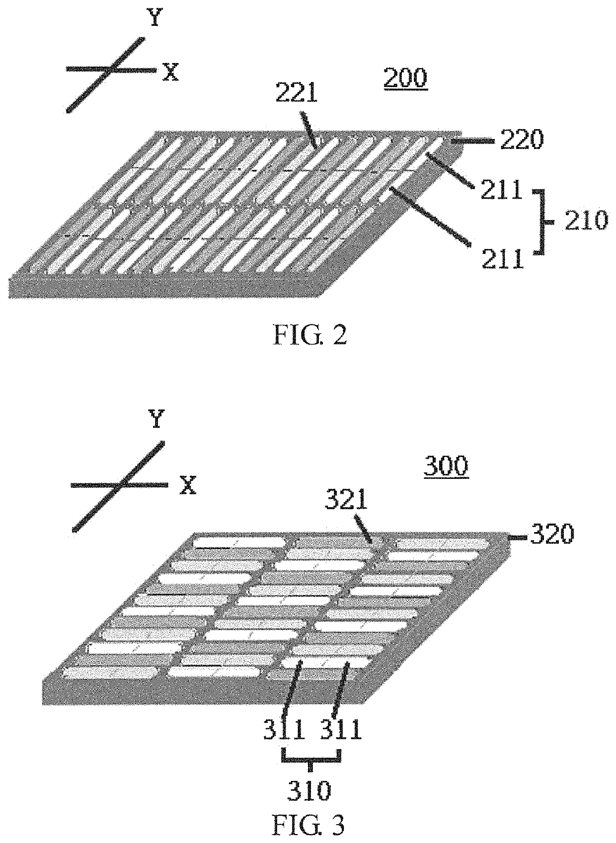
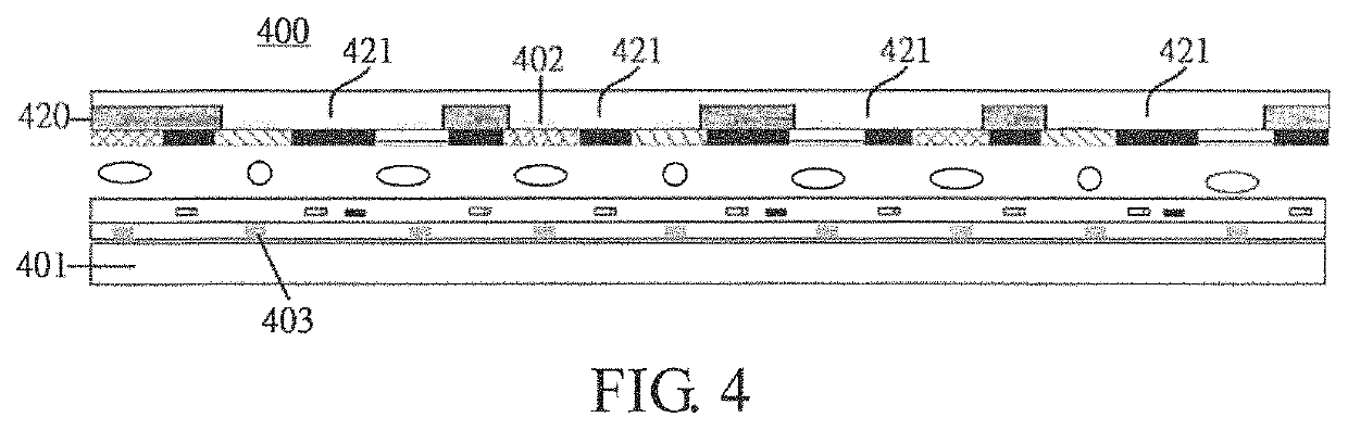
[0026]In order to solve the problem of inaccurate pixel printing when preparing a conventional panel, there is an urgent need to develop a novel pixel design that can improve the success rate of printing, which has a larger opening of the pixel ...


PUM


Abstract

The present invention provides a display including: a pixel definition layer having a plurality of strip-shaped openings arranged in at least two columns or at least two rows parallel to each other; and a plurality of sub-pixels, wherein at least two adjacent sub-pixels are disposed in each of the strip-shaped openings.

Description

BACKGROUND OF INVENTIONField of Invention[0001]The present invention relates to a display, and more particularly to a display having a strip-shaped pixel definition layer.Description of Prior Art[0002]An inkjet printing method can efficiently utilize materials and is suitable for preparing large-area display panels. Referring to FIG. 1, FIG. 1 is a schematic diagram of a pixel design of a conventional panel 100 commonly used, which is a side-by-side (SBS) design, that is, each pixel 110 is made of independent sub-pixels 111 regularly arranged. The sub-pixels 111 are spaced apart from each other by a pixel definition layer 120. In general, inkjet printed pixels have sizes of approximately 200 um*200 um (depending on the screen size and resolution), and the sub-pixel requirements are required even to be smaller, and ink drops of the inkjet printing have diameters of approximately 30 um. For the inkjet printing, printing such pixels requires the printer to have extremely high printing ...

Claims


Application Information

Patent Timeline
Patent Type & Authority Patents(United States)
IPC IPC(8): H01L29/08H01L27/32H01L51/00H01L51/56
CPCH01L27/3246H01L51/0005H01L51/56H10K59/122H10K71/135H10K71/00H10K59/35
Inventor LI, XIANGLONGMENG, HONG
Owner SHENZHEN CHINA STAR OPTOELECTRONICS SEMICON DISPLAY TECH CO LTD
Why Eureka
Try Eureka