Supercharge Your Innovation With Domain-Expert AI Agents!

Display panel and manufacturing method thereof

a technology of display panels and manufacturing methods, applied in the field of display panels, can solve the problems of poor brightness uniformity at different locations of large-sized oled display panels, and achieve the effects of good grid continuity, high accuracy, and good continuity

Active Publication Date: 2021-11-02
SHENZHEN CHINA STAR OPTOELECTRONICS SEMICON DISPLAY TECH CO LTD
View PDF14 Cites 0 Cited by
  • Summary
  • Abstract
  • Description
  • Claims
  • Application Information

AI Technical Summary

Benefits of technology

The method effectively reduces resistance voltage drops and enhances brightness uniformity across large-sized OLED display panels by creating a patterned nucleation inhibiting layer using laser ablation, ensuring good grid continuity and high accuracy in the conductive layer formation.

Problems solved by technology

For large-size OLED display panels, the common cathode surface resistance is high, and there will be a serious power voltage drop (IR-drop), resulting in poor brightness uniformity at different locations of the large-sized OLED display panels.

Method used


Image

  • Display panel and manufacturing method thereof
  • Display panel and manufacturing method thereof
  • Display panel and manufacturing method thereof

Examples


Embodiment Construction

[0045]The technical solutions in the embodiments of the present invention will be clearly and completely described below with reference to the drawings in the embodiments of the present invention. Obviously, the described embodiments are only a part of the embodiments of the present invention, but not all the embodiments. Based on the embodiments in the present invention, all other embodiments obtained by those skilled in the art without creative work fall into the scope of the present invention.

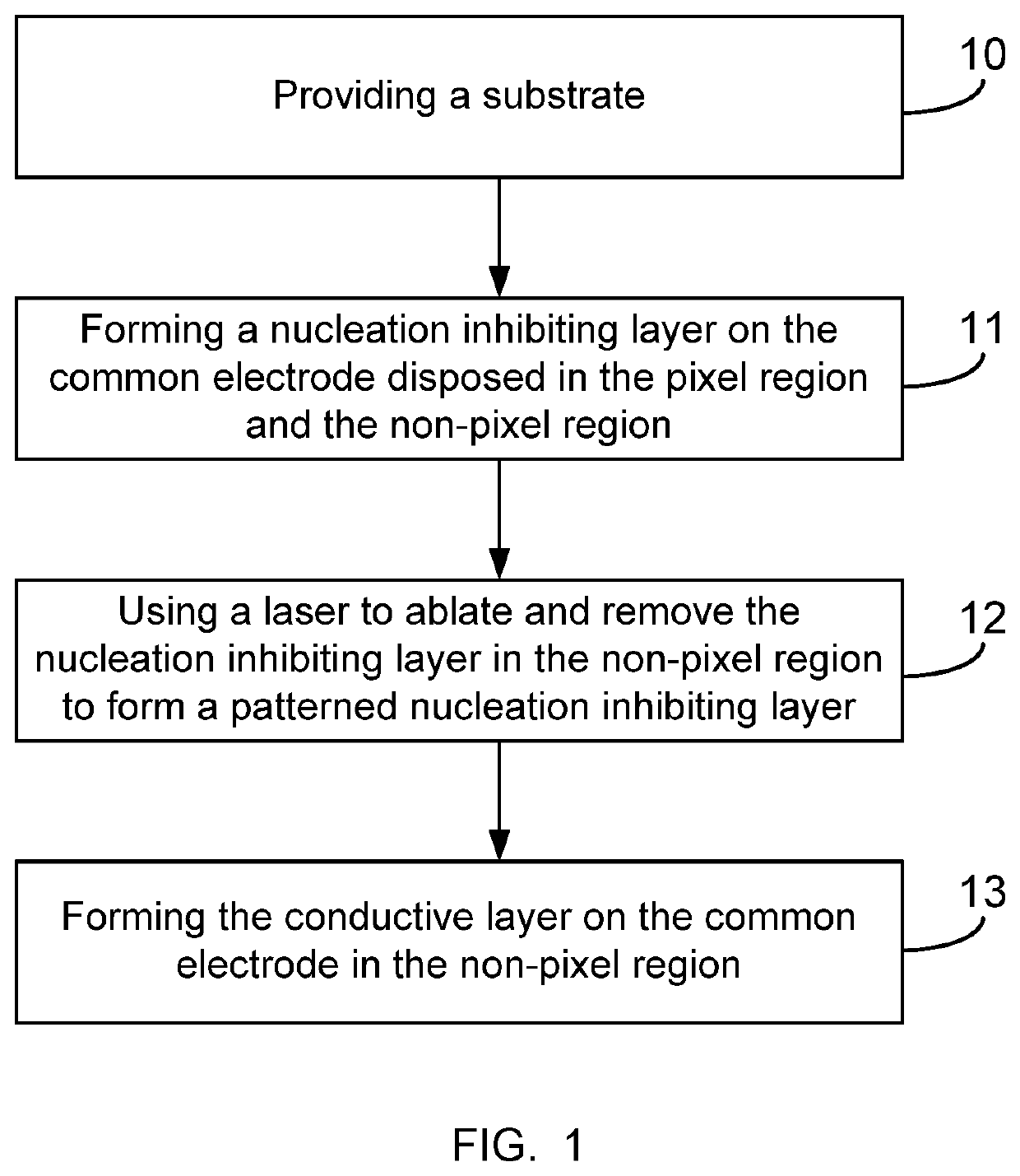
[0046]Please refer to FIG. 1, which is a flowchart of a manufacturing method of a display panel according to an embodiment of the present invention. The manufacturing method of the display panel comprises following steps of:

[0047]S10: providing a substrate.

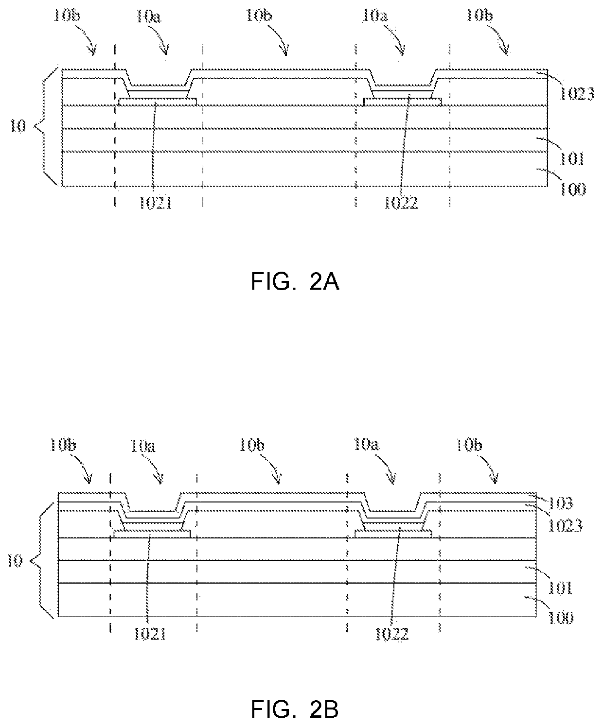
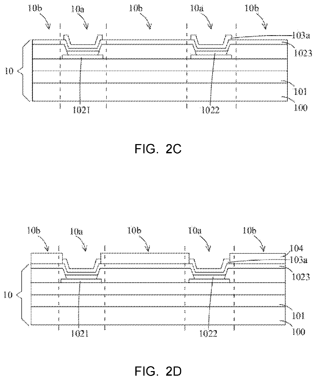
[0048]Specifically, as shown in FIG. 2A, the substrate 10 is an organic light emitting diode array substrate. The substrate 10 comprises a pixel region 10a and a non-pixel region 10b disposed outside the pixel region 10a. The substrate 10 ...


PUM

PropertyMeasurementUnit
thicknessaaaaaaaaaa
wavelengthaaaaaaaaaa
thicknessesaaaaaaaaaa

Abstract

The present invention provides a display panel and a manufacturing method thereof. By using a laser ablation to form a patterned nucleation inhibiting layer with good grid continuity and high accuracy, and using a nucleation inhibiting layer to inhibit a conductive layer from being formed on a surface of the nucleation inhibiting layer and to form the conductive layer with good continuity on a common electrode in a non-pixel region, thereby improving a resistance voltage drop of a cathode formed by the common electrode and the conductive layer, and improving uniformity of brightness of a display on the display panel.

Description

[0001]This application claims the priority of a Chinese patent application filed on Oct. 30, 2019 with the Chinese Patent Office, Application number as: 201911042322.1, and the title of the invention as “display panel and manufacturing method thereof.” The entire contents of which are incorporated herein by reference.FIELD OF INVENTION[0002]The present application relates to the field of display technology, and in particular, to a display panel and a manufacturing method thereof.BACKGROUND OF INVENTION[0003]Organic light emitting display (OLED) devices have advantages such as self-luminous, all-solid-state, low driving voltages, high luminous efficiency, short response time, high sharpness and contrast, near 180° viewing angle, wide operating temperature ranges, and can realize flexible display and full color display with large areas, and are recognized as the most promising display devices by industries.[0004]At present, applications of small-sized OLEDs in mobile smart terminals a...

Claims


Application Information

Patent Timeline
Patent Type & Authority Patents(United States)
IPC IPC(8): H01L21/00H01L51/52H01L51/56H01L27/32
CPCH01L51/5228H01L51/5253H01L51/5275H01L51/56H01L27/3244H10K59/12H10K59/1201H10K59/875H10K59/873H10K59/80522H10K71/621H10K2102/351H10K50/824H10K50/844H10K50/858H10K71/00
Inventor TAN, WEILI, JINCHUAN
Owner SHENZHEN CHINA STAR OPTOELECTRONICS SEMICON DISPLAY TECH CO LTD
Features
  • R&D
  • Intellectual Property
  • Life Sciences
  • Materials
  • Tech Scout
  • Unparalleled Data Quality
  • Higher Quality Content
  • 60% Fewer Hallucinations
Learn More