Semiconductor, semiconductor device, and method for fabricating the same

a semiconductor and semiconductor technology, applied in the direction of crystal growth process, gel state, polycrystalline material growth, etc., can solve the problems of inability to achieve crystal growth progress, large amount of energy required, and conventional solid phase epitaxial crystallization did not provide an answer to this problem, etc., to achieve excellent crystallinity, increase temperature, and shorten the time necessary for crystal growth

Inactive Publication Date: 2006-02-14
SEMICON ENERGY LAB CO LTD
View PDF133 Cites 60 Cited by
  • Summary
  • Abstract
  • Description
  • Claims
  • Application Information

AI Technical Summary

Benefits of technology

[0016]In particular, by setting the material containing nickel, iron, cobalt, platinum or palladium selectively, it is possible to control the direction of the crystal growth. Because, unlike crystalline silicon produced by conventional solid phase epitaxial growth, crystalline silicon obtained using this kind of technique has a structure in which the continuity of the crystallinity over long distances is good and which is close to being monocrystalline, it is well suited to use in semiconductor devices such as TFTs.
[0017]In the present invention, nickel, iron, cobalt, platinum or palladium is used. These materials are not desirable for silicon which is used as a semiconductor material. If such a material is contained excessively in the silicon film, it is necessary to remove the material. With respect to nickel, when a growing crystal of nickel silicide arrives its final points, i.e., the crystallization has been completed, as a result of the above-described reaction, the nickel silicide is easily dissolved in hydrofluoric acid or hydrochloric acid. The nickel contained in the substrate can be reduced by treating the nickel with these acids.

Problems solved by technology

However, with this kind of method, at temperatures below 600° C. almost no crystal growth progress has occurred.
However, in this process a large amount of energy is required for cutting the first molecule chains and maintaining the state wherein these cut molecules do not combine with other molecules, and this has been a barrier in the crystallization reaction.
The idea of conventional solid phase epitaxial crystallization did not provide an answer to this problem.

Method used


Image

  • Semiconductor, semiconductor device, and method for fabricating the same
  • Semiconductor, semiconductor device, and method for fabricating the same
  • Semiconductor, semiconductor device, and method for fabricating the same

Examples


example 1

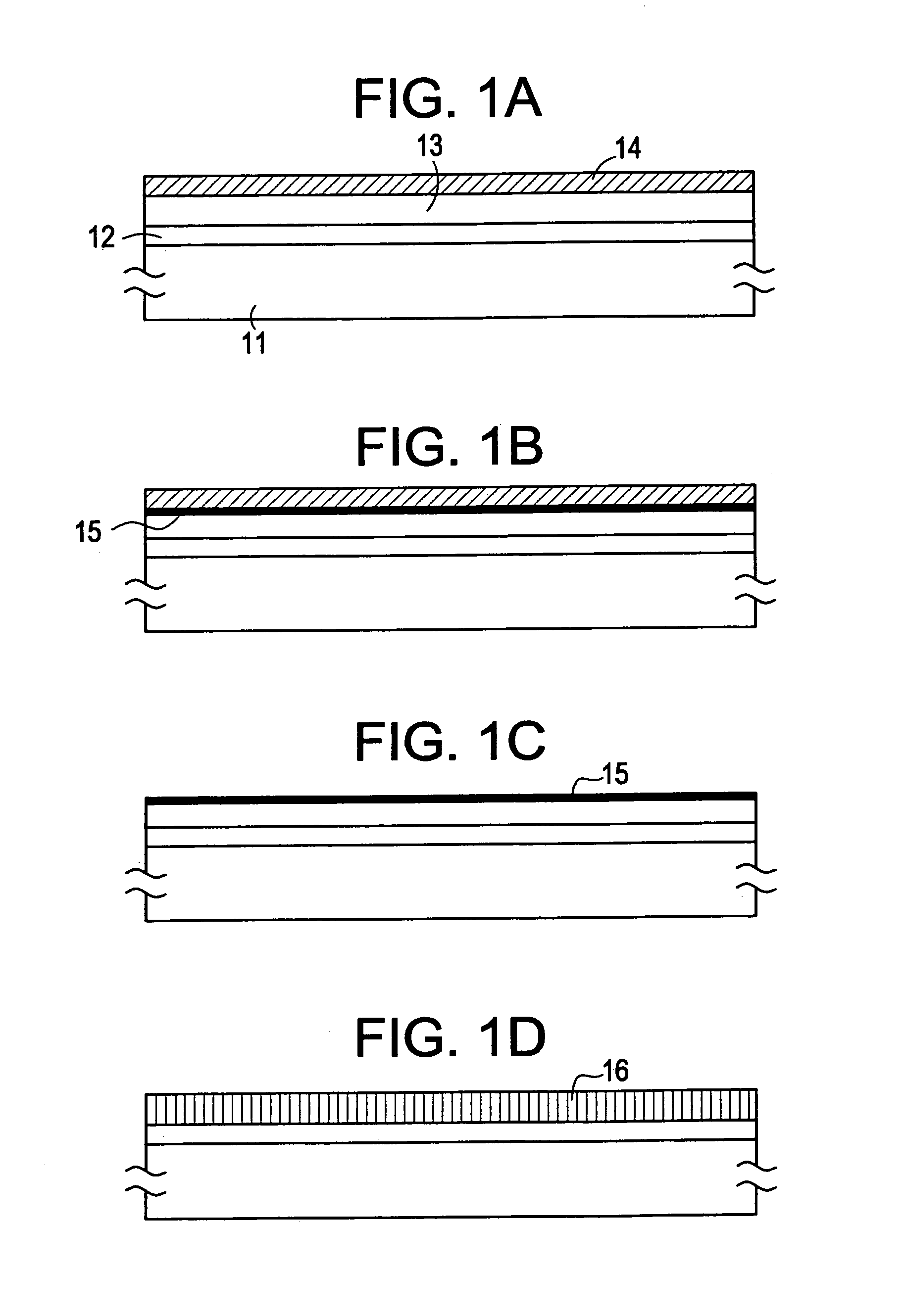
[0053]Referring to FIG. 1, a process for fabricating a crystalline silicon film by forming a nickel film on a Corning #7059 substrate, and crystallizing an amorphous silicon film using this nickel film is described below. By using plasma CVD, a 2,000 Å thick silicon oxide film 12 as a base film was deposited on the substrate 11, and further thereon an amorphous silicon film 13 at a thickness of from 500 to 3,000 Å, for example, at a thickness of 1,500 Å. After removing hydrogen from the film by keeping the film at a temperature of 430° C. for a duration of from 0.1 to 2 hours, for example, 0.5 hour, a nickel film 14 was deposited thereon by sputtering at a thickness of from 100 to 1,000 Å, for example, 500 Å. A favorable nickel film can be obtained by heating the substrate in the temperature range of from 100 to 500° C., preferably in the range of from 180 to 250° C., because a nickel film having an improved adhesion strength with respect to the silicon film formed as the base is ob...

example 2

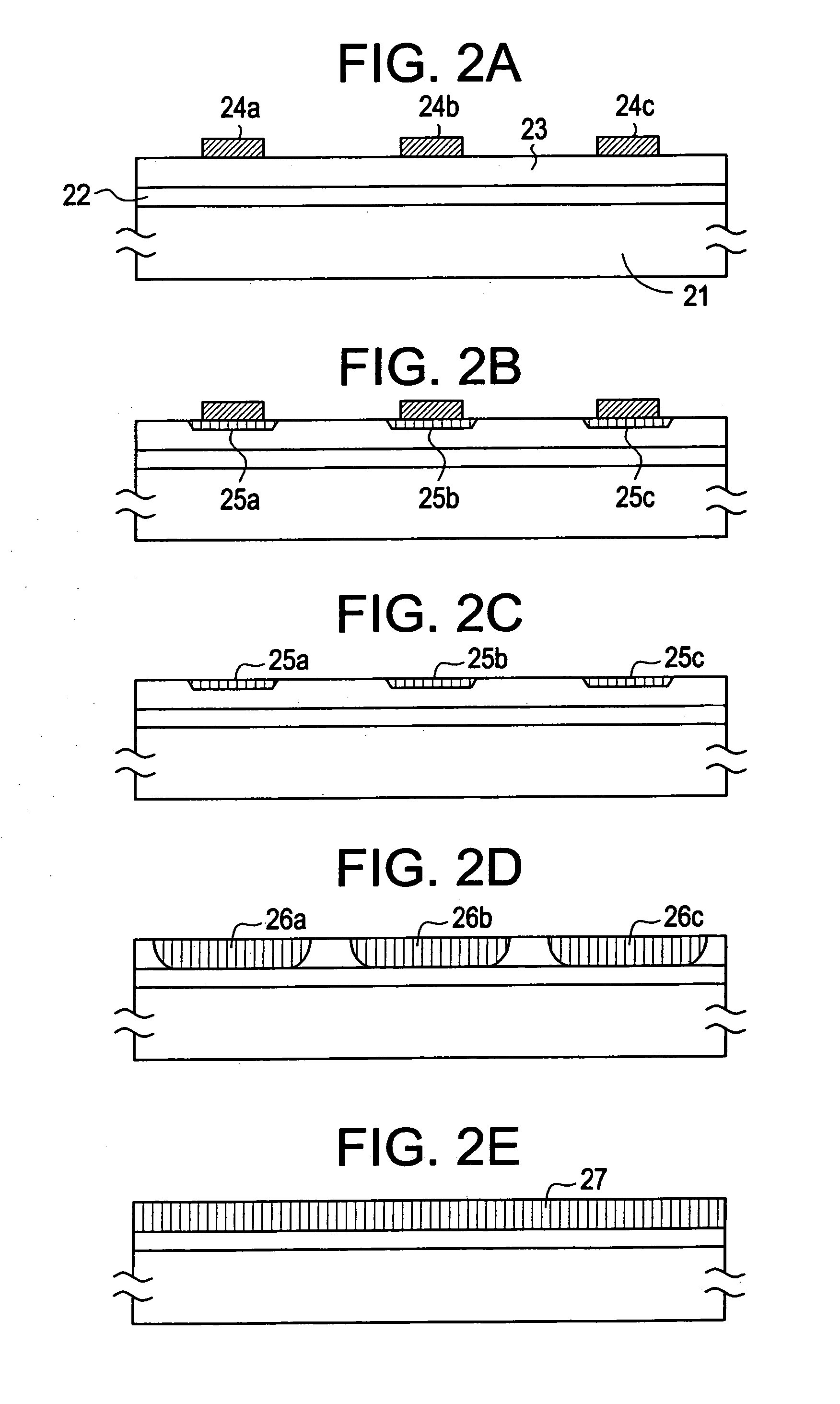
[0057]Referring to FIG. 2, a process for fabricating a crystalline silicon film is described below. A 2,000 Å thick silicon oxide film 22 as a base film was deposited on a Corning #7059 glass substrate 21, and an amorphous silicon film 23 was deposited further thereon at a thickness of from 500 to 3,000 Å, for example, at a thickness of 500 Å and 1,500 Å. After removing hydrogen from the film by keeping the film at a temperature of 430° C. for a duration of from 0.1 to 2 hours, for example, 0.5 hour, a nickel film was deposited thereon by sputtering at a thickness of from 100 to 1,000 Å, for example, 500 Å. A nickel silicide film can be used in the place of the nickel film. The nickel film thus obtained was etched to form patterns 24a, 24b, and 24c as shown in FIG. 2(A).

[0058]Then, the structure was heated in the temperature range of from 450 to 580° C. for a duration of from 1 to 10 minutes to allow the nickel films 24a to 24c to undergo reaction with the amorphous film 23 to form ...

example 3

[0063]The present example relates to a process for fabricating a silicon film having an improved crystallinity by irradiating a laser beam to the silicon film after once crystallizing it by heating. Furthermore, the present example provides a process for fabricating a TFT using the thus crystallized silicon film.

[0064]FIG. 6 shows the cross section view of the step-sequential structures obtained in the present process. Referring to FIG. 6, a 2,000 Å thick silicon oxide film 602 as a base film was deposited on a Corning #7059 glass substrate 601, and an intrinsic (I type) amorphous silicon film was deposited further thereon at a thickness of from 100 to 1,500 Å, for example, at a thickness of 800 Å in this case. A nickel film, i.e., a catalytic material for accelerating the crystallization of the amorphous silicon, was deposited selectively thereon by a process similar to that described in Example 2 (refer to FIG. 2(A)). The resulting structure was then heated in the temperature rang...


PUM

PropertyMeasurementUnit
temperatureaaaaaaaaaa

Abstract

Method of fabricating semiconductor devices such as thin-film transistors by annealing a substantially amorphous silicon film at a temperature either lower than normal crystallization temperature of amorphous silicon or lower than the glass transition point of the substrate so as to crystallize the silicon film. Islands, stripes, lines, or dots of nickel, iron, cobalt, or platinum, silicide, acetate, or nitrate of nickel, iron, cobalt, or platinum, film containing various salts, particles, or clusters containing at least one of nickel, iron, cobalt, and platinum are used as starting materials for crystallization. These materials are formed on or under the amorphous silicon film.

Description

[0001]This application is a Continuation of Ser. No. 08 / 481,062, filed Jun. 7, 1995, now abandoned; which itself is a Continuation-in-Part of Ser. No. 08 / 196,856, filed Feb. 15, 1994 now U.S. Pat. No. 5,639,698.BACKGROUND OF THE INVENTION[0002]This invention relates to a method for obtaining crystalline semiconductors for use in thin film devices such as thin film insulator gate type field effect transistors (Thin Film Transistors, or TFTs).[0003]Conventionally, crystalline silicon semiconductor thin films used in thin film devices such as thin film insulator gate type field effect transistors (TFTs) have been manufactured by forming an amorphous silicon film on an insulating surface such as an insulator substrate by plasma CVD or thermal CVD and then crystallizing this film in an electric furnace or the like at a temperature of above 600° C. over a long period of twelve hours or more. In order to obtain particularly good performance (high field effect mobility and high reliability)...

Claims


Application Information

Patent Timeline
Patent Type & Authority Patents(United States)
IPC IPC(8): C30B1/06H01L21/20H01L21/336H01L21/77H01L21/84H01L29/786
CPCH01L21/2026H01L29/66757H01L27/1277H01L29/78696H01L29/78618H01L21/02422H01L21/02488H01L21/02532H01L21/02672H01L21/02686
Inventor YAMAZAKI, SHUNPEITAKEMURA, YASUHIKOZHANG, HONGYONGTAKAYAMA, TORUUOCHI, HIDEKI
Owner SEMICON ENERGY LAB CO LTD
Why Eureka
Try Eureka