Wafer chuck apparatus, method for measuring wafer bow value and semiconductor process flow

a wafer chuck and wafer bow technology, applied in the direction of fluid tightness measurement, semiconductor/solid-state device testing/measurement, instruments, etc., can solve the problem of poor chip yield, and achieve the effect of reducing the risk of defective products and improving yield

Active Publication Date: 2022-03-22
POWERCHIP SEMICON MFG CORP
View PDF10 Cites 0 Cited by
  • Summary
  • Abstract
  • Description
  • Claims
  • Application Information

AI Technical Summary

Benefits of technology

[0011]The disclosure provides a measuring method for converting a gas leak rate to a wafer bow value, which is relatively simpler and faster.
[0015]Based on the above, in the method of measuring wafer bow value of the disclosure, the wafer bow value of the wafer on the wafer chuck apparatus can be estimated by the leak rates of the plurality of passageway pairs in the process. Therefore, the method of measuring wafer bow value of the embodiment may be made simpler and faster.
[0016]The disclosure provides a semiconductor process flow that can reduce the risk of defective products or improve yield.
[0019]Based on the above, in the semiconductor process flow of the disclosure, it is possible to determine whether or not the semiconductor process can be performed by the estimated wafer bow value. Therefore, the yield of the semiconductor process flow can be improved.

Problems solved by technology

Because the wafer bow value of the wafer may cause abnormal film thickness, the yield of the chips is not good.

Method used


Image

  • Wafer chuck apparatus, method for measuring wafer bow value and semiconductor process flow
  • Wafer chuck apparatus, method for measuring wafer bow value and semiconductor process flow
  • Wafer chuck apparatus, method for measuring wafer bow value and semiconductor process flow

Examples


Embodiment Construction

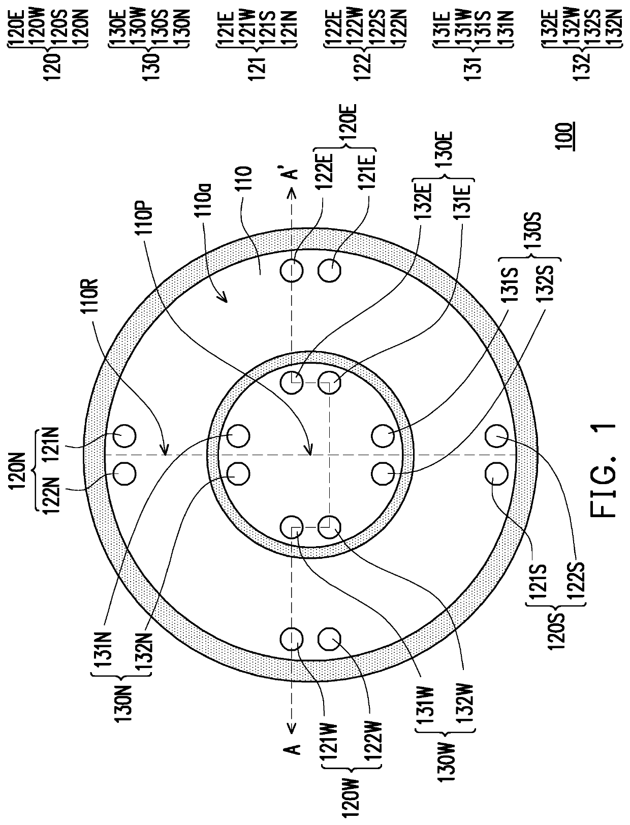
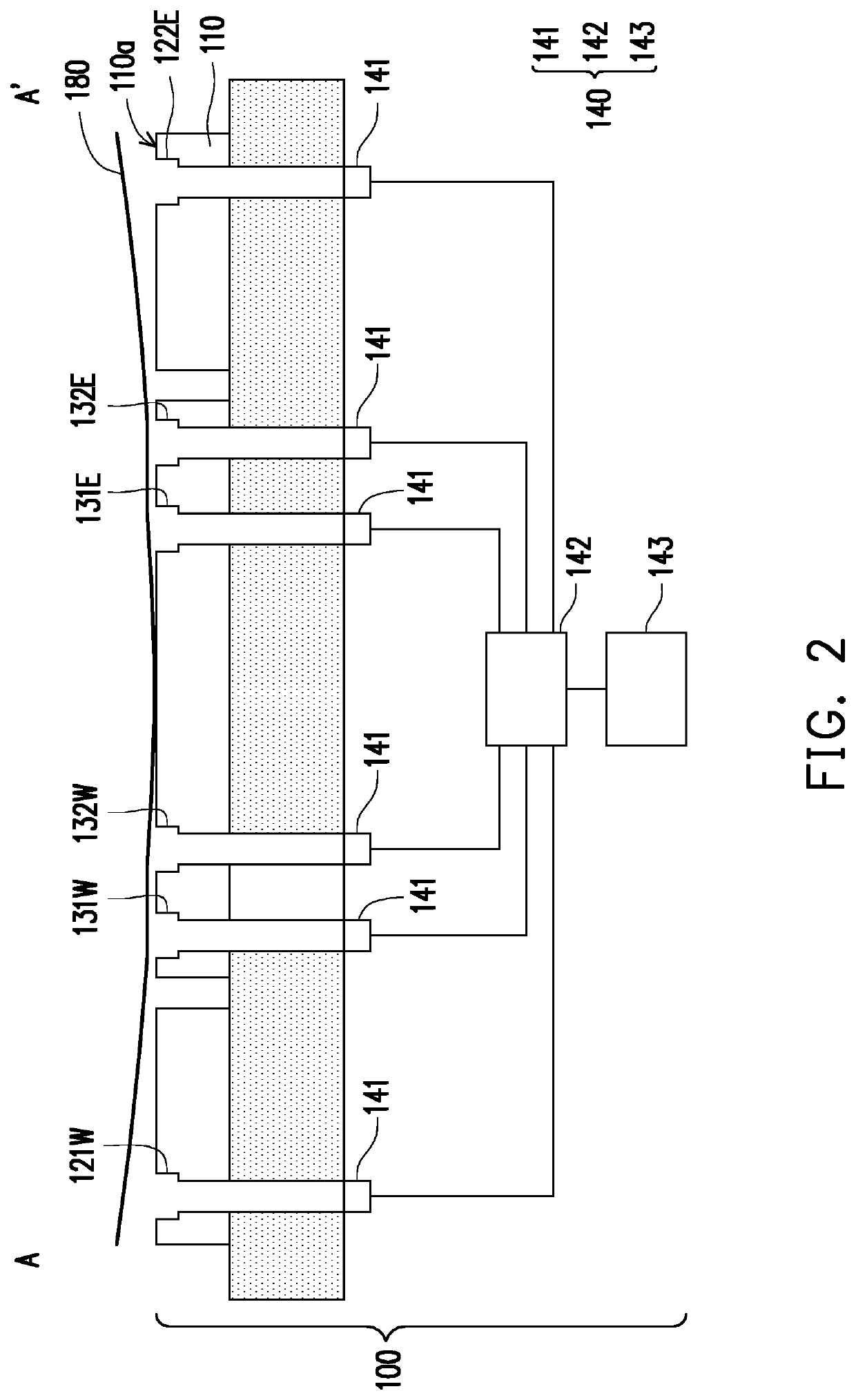
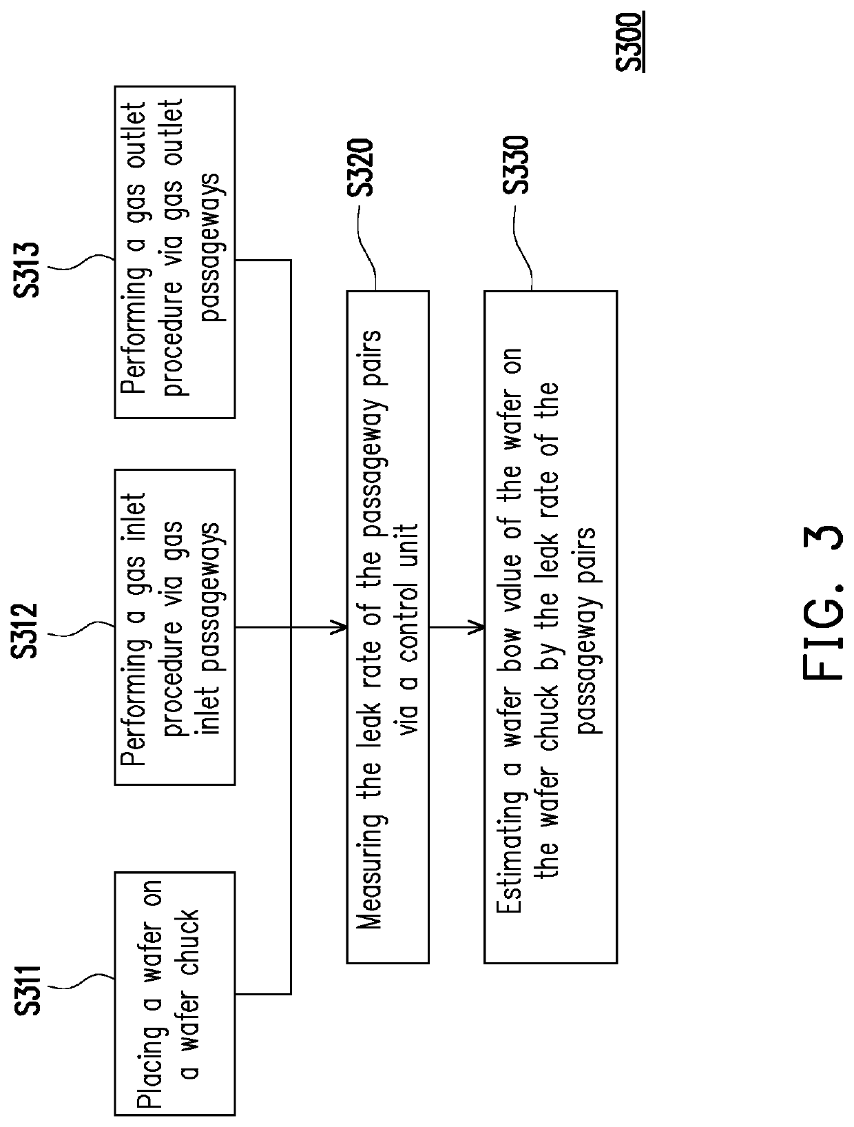
[0028]The embodiments are described in detail below with reference to the drawings, but the embodiments are not intended to limit the scope of the description. In addition, the drawings are for illustrative purposes only and may be not drawn to the original dimensions. For easier understanding, the same elements in the following description will be denoted by the same reference numerals. In addition, the terms “comprising”, “including”, “having”, “comprise”, “include”, “have”, etc. used in the description are inclusive or open-ended and do not exclude additional, unrecited elements or method steps. In addition, the terms “substantially”, “approximately”, “about” and the like used in the description may include an acceptable tolerance range. Moreover, the directional terms mentioned in the description, such as “upper” and “lower”, are only used to refer to the direction of the figure. Therefore, the directional terminology used is for the purpose of illustration and not limitation.

[0...


PUM


Abstract

A method for measuring wafer bow value comprising the following steps is provided. Place a wafer on a wafer chuck apparatus. A gas inlet process is performed on gas inlet passageways of a passageway pair of the wafer chuck apparatus. A gas outlet process is performed on gas outlet passageways of a passageway pair of the wafer chuck apparatus. A leak rate of each channel pair is measured by the control unit when the wafer is placed on the wafer chuck apparatus and during the gas inlet process and gas outlet process are performed. A wafer bow value of the wafer on the wafer chuck apparatus is estimated by the leak rate of the passageway pair. A wafer chuck apparatus is provided. A semiconductor process flow is provided.

Description

CROSS-REFERENCE TO RELATED APPLICATION[0001]This application claims the priority benefit of Taiwan application serial no. 108108150, filed on Mar. 12, 2019. The entirety of the above-mentioned patent application is hereby incorporated by reference herein and made a part of this specification.BACKGROUNDTechnical Field[0002]The disclosure relates to a semiconductor device, a semiconductor measurement method, and a process flow, and more particular, a wafer chuck apparatus, a method for measuring wafer bow value, and a semiconductor process flow.Description of Related Art[0003]At present, the wafer bow value of the wafer can only be measured by random sampling. Because the wafer bow value of the wafer may cause abnormal film thickness, the yield of the chips is not good. Therefore, how to quickly estimate the wafer bow value of the wafer under the time conditions that affect the output can quickly and effectively improve the process yield.SUMMARY[0004]The disclosure provides a wafer ch...

Claims


Application Information

Patent Timeline
Patent Type & Authority Patents(United States)
IPC IPC(8): H01L21/66H01L21/67G01M3/32
CPCH01L21/67253G01M3/3254H01L21/67288H01L22/12H01L21/68785H01L21/67276
Inventor TSAI, CHENG-YENCHEN, WEI-SHENG
Owner POWERCHIP SEMICON MFG CORP
Why Eureka
Try Eureka