FPC connector, touch-sensitive screen and display device
a touch-sensitive screen and display device technology, applied in the field of connectors, can solve the problems of inability to accommodate more pins, large waste, inconvenience in maintenance, etc., and achieve the effects of large waste, easy subjection, and non-reusability
- Summary
- Abstract
- Description
- Claims
- Application Information
AI Technical Summary
Benefits of technology
Problems solved by technology
Method used
Image
Examples
embodiment 1
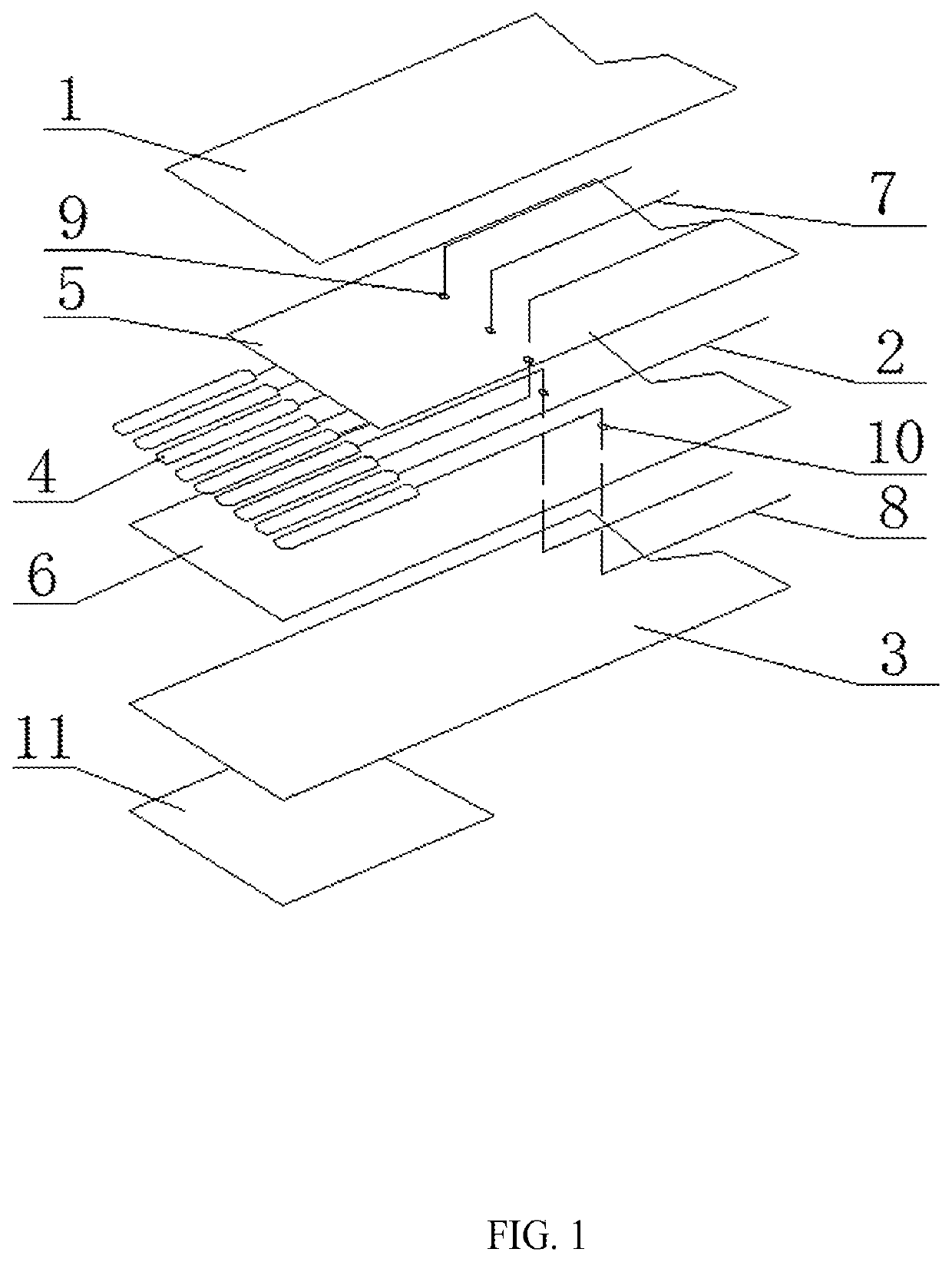
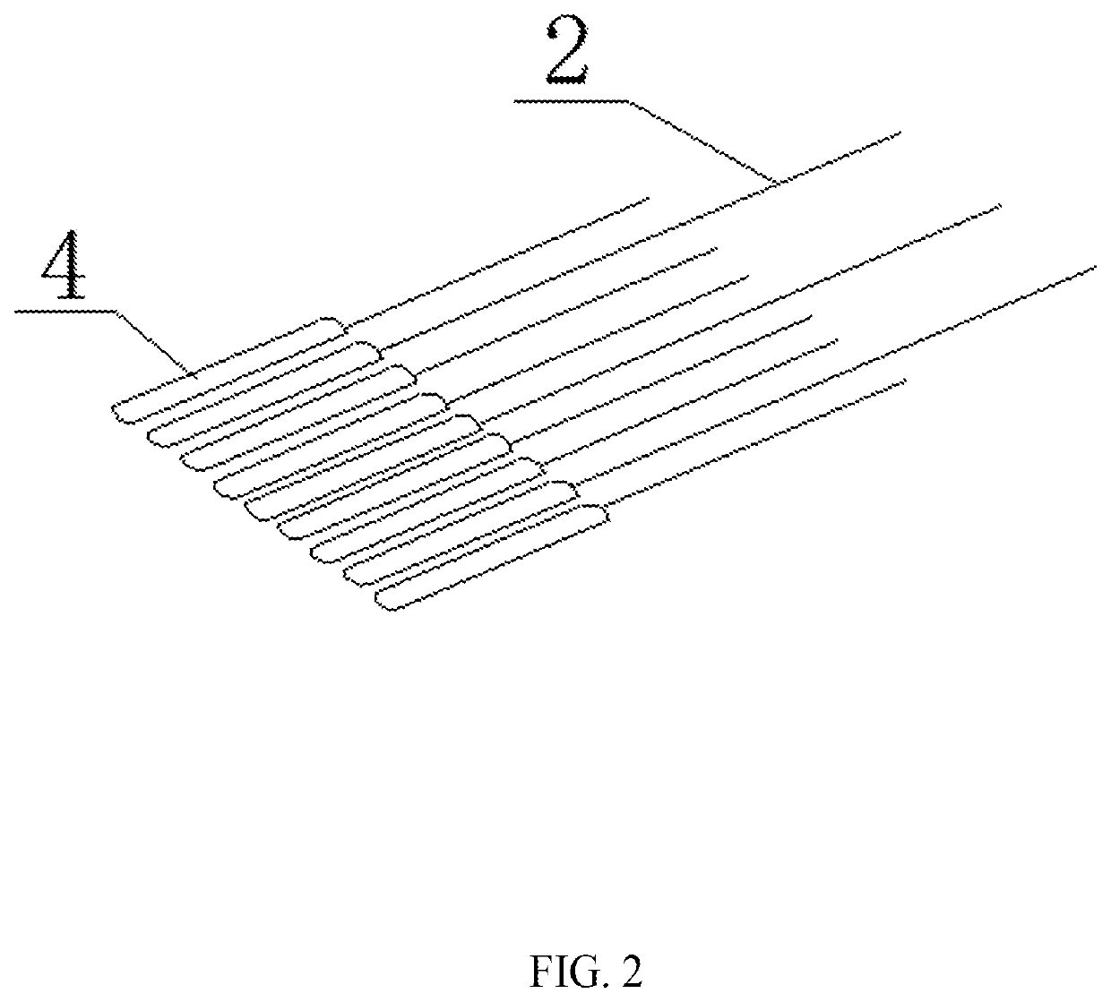
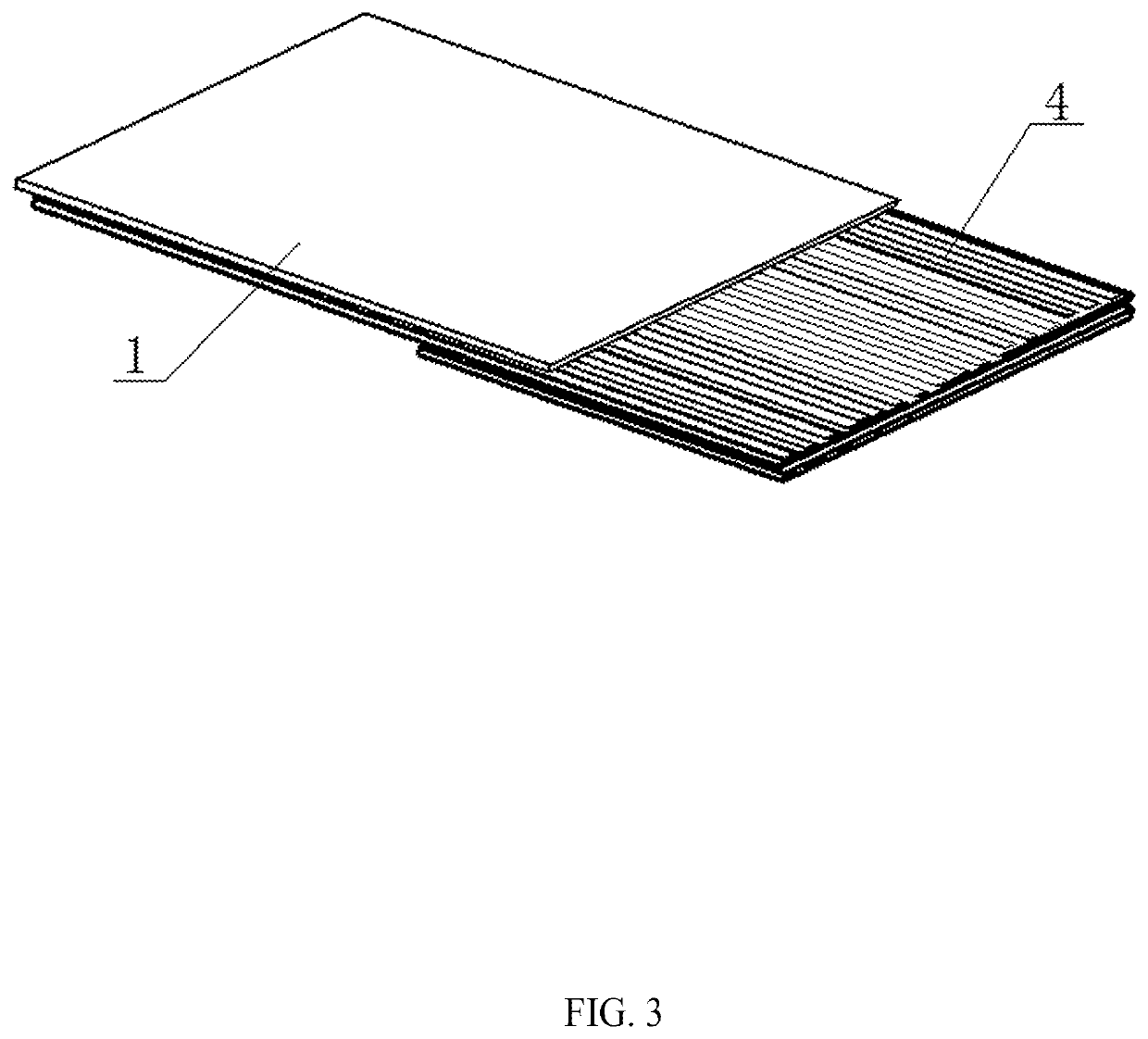
[0047]As shown in FIGS. 1 to 3, an FPC connector is provided, comprising a first insulating layer 1, a first circuit layer 2 and a second insulating layer 3. The first circuit layer 2 is located at an underside of the first insulating layer 1, and the second insulating layer 3 is located at an underside of the first circuit layer 2. The first circuit layer 2 and the second insulating layer 3 each has a forepart extending beyond a front end of the first insulating layer 1. The first circuit layer 2 comprises a plurality of conductive strips having foreparts arranged in parallel at equal intervals. A metal layer 4 is plated with or deposited on the foreparts of the first circuit layer 2. The metal layer 4 and the foreparts of the first circuit layer 2 constitute metal fingers.
[0048]The first insulating layer 1 and the second insulating layer 3 insulate and protect the first circuit layer 2. High routing density, lightweight, slimness, and flexibility of the first insulating layer 1, t...
embodiment 2
[0058]FIG. 4 shows an alternative embodiment of the FPC connector that is similar to the FPC connector of embodiment 1. They differ in that the fourth insulating layers 6 and the third circuit layers 8 are omitted in the present embodiment. Specifically, the FPC connector includes a first insulating layer 1, a first circuit layer 2, a second insulating layer 3, a third insulating layer 5, and a second circuit layer 7. The first circuit layer 2 is arranged between the first insulating layer 1 and the second insulating layer 3. The first circuit layer 2 includes a number of conductive strips. The third insulating layer 5 is arranged between the first insulating layer 1 and the first circuit layer 2. The second circuit layer 7 includes a number of conductive strips that are provided on an upper side face of the third insulating layer 5. Ends of the plurality of conductive strips of the second circuit layer 7 pass through the third insulating layer 5 and are correspondingly connected to...
embodiment 3
[0060]FIG. 5 shows an alternative embodiment of the FPC connector that is similar to the FPC connector of embodiment 1. They differ in that the fourth insulating layers 6 and the third circuit layers 8 are omitted in the present embodiment. Specifically, the FPC connector includes a first insulating layer 1, a first circuit layer 2, a second insulating layer 3, a third insulating layer 5, a second circuit layer 7, and a reinforcing plate 11a. The first circuit layer 2 is arranged between the first insulating layer 1 and the second insulating layer 3. The first circuit layer 2 includes a number of conductive strips. The third insulating layer 5 is arranged between the first insulating layer 1 and the first circuit layer 2. The second circuit layer 7 includes a number of conductive strips that are provided on an upper side face of the third insulating layer 5. Ends of the plurality of conductive strips of the second circuit layer 7 pass through the third insulating layer 5 and are cor...
PUM
| Property | Measurement | Unit |
|---|---|---|
| distance | aaaaa | aaaaa |
| distance | aaaaa | aaaaa |
| conductive | aaaaa | aaaaa |
Abstract
Description
Claims
Application Information


