FPC connector, touch-sensitive screen and display device
- Summary
- Abstract
- Description
- Claims
- Application Information
AI Technical Summary
Benefits of technology
Problems solved by technology
Method used
Image
Examples
embodiment 1
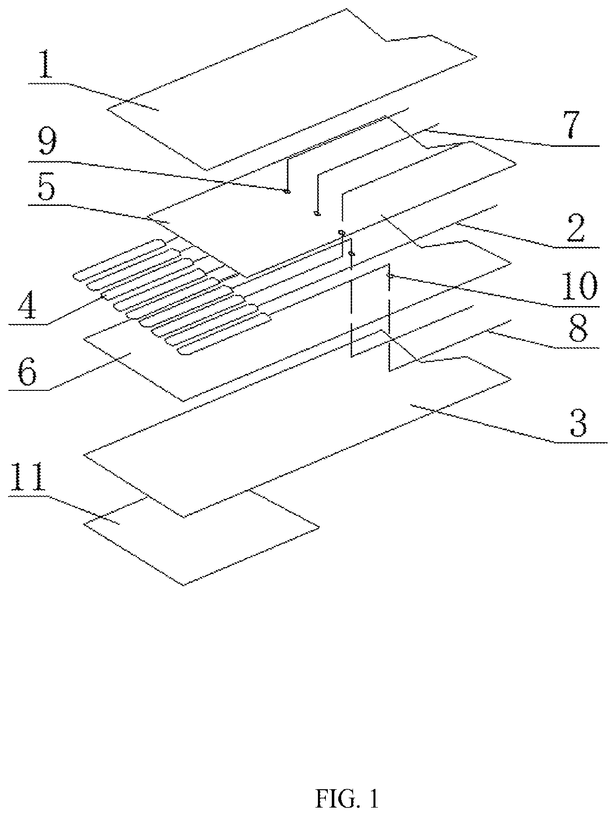
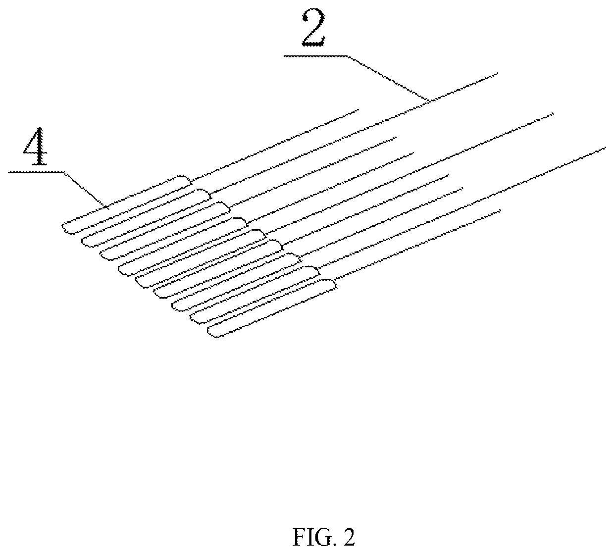
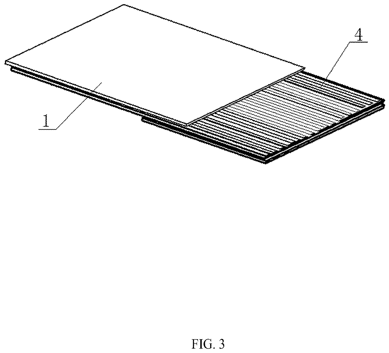
[0047]As shown in FIGS. 1 to 3, an FPC connector is provided, comprising a first insulating layer 1, a first circuit layer 2 and a second insulating layer 3. The first circuit layer 2 is located at an underside of the first insulating layer 1, and the second insulating layer 3 is located at an underside of the first circuit layer 2. The first circuit layer 2 and the second insulating layer 3 each has a forepart extending beyond a front end of the first insulating layer 1. The first circuit layer 2 comprises a plurality of conductive strips having foreparts arranged in parallel at equal intervals. A metal layer 4 is plated with or deposited on the foreparts of the first circuit layer 2. The metal layer 4 and the foreparts of the first circuit layer 2 constitute metal fingers.
[0048]The first insulating layer 1 and the second insulating layer 3 insulate and protect the first circuit layer 2. High routing density, lightweight, slimness, and flexibility of the first insulating layer 1, t...
embodiment 2
[0058]FIG. 4 shows an alternative embodiment of the FPC connector that is similar to the FPC connector of embodiment 1. They differ in that the fourth insulating layers 6 and the third circuit layers 8 are omitted in the present embodiment. Specifically, the FPC connector includes a first insulating layer 1, a first circuit layer 2, a second insulating layer 3, a third insulating layer 5, and a second circuit layer 7. The first circuit layer 2 is arranged between the first insulating layer 1 and the second insulating layer 3. The first circuit layer 2 includes a number of conductive strips. The third insulating layer 5 is arranged between the first insulating layer 1 and the first circuit layer 2. The second circuit layer 7 includes a number of conductive strips that are provided on an upper side face of the third insulating layer 5. Ends of the plurality of conductive strips of the second circuit layer 7 pass through the third insulating layer 5 and are correspondingly connected to...
embodiment 3
[0060]FIG. 5 shows an alternative embodiment of the FPC connector that is similar to the FPC connector of embodiment 1. They differ in that the fourth insulating layers 6 and the third circuit layers 8 are omitted in the present embodiment. Specifically, the FPC connector includes a first insulating layer 1, a first circuit layer 2, a second insulating layer 3, a third insulating layer 5, a second circuit layer 7, and a reinforcing plate 11a. The first circuit layer 2 is arranged between the first insulating layer 1 and the second insulating layer 3. The first circuit layer 2 includes a number of conductive strips. The third insulating layer 5 is arranged between the first insulating layer 1 and the first circuit layer 2. The second circuit layer 7 includes a number of conductive strips that are provided on an upper side face of the third insulating layer 5. Ends of the plurality of conductive strips of the second circuit layer 7 pass through the third insulating layer 5 and are cor...
PUM
 Abstract
Description
Claims
Application Information


