Semiconductor package substrate having heat dissipating metal sheet on solder pads, method for fabricating the same, and electronic package having the same

a technology of semiconductor and package substrate, which is applied in the direction of semiconductor/solid-state device details, electrical equipment, semiconductor devices, etc., can solve the problems of poor heat dissipation efficiency of the package substrate, affecting the overall performance, and reducing the transmission speed and calculation speed, so as to ensure the overall performance and lifespan of the electronic package, and avoid overheating the entire electronic package

Active Publication Date: 2022-09-20
PHOENIX PIONEER TECH
View PDF6 Cites 0 Cited by
  • Summary
  • Abstract
  • Description
  • Claims
  • Application Information

AI Technical Summary

Benefits of technology

[0018]It is known from the above that in the semiconductor package substrate, the method for fabricating the same, and the electronic package having the same according to the present disclosure, the insulation layer is not formed in the first hole of the metal sheet, and the first conductive element that is used to be grounded can be in contact with the metal sheet. Therefore, the heat generated during a signal transmission process can be dissipated not only by the metal material and dielectric material of the semiconductor package substrate, but also by the metal sheet and the first conductive element. Compared with the prior art, the present disclosure prevents the heat from being accumulated in the semiconductor package substrate, so as to avoid overheating the entire electronic package. Therefore, the semiconductor package substrate meets the heat dissipating requirement, which ensures the overall performance and lifespan of the electronic package.

Problems solved by technology

However, the heat dissipating efficiency of the package substrate 1a is poor, and the heat will accumulate in the package substrate 1a, which heats up the whole electronic package 1 and affects the overall performance (e.g., reducing the transmission speed and calculation speed) and lifespan of the electronic package 1.
Therefore, how to solve the problems of the prior art is becoming an urgent issue in the art.

Method used


Image

  • Semiconductor package substrate having heat dissipating metal sheet on solder pads, method for fabricating the same, and electronic package having the same
  • Semiconductor package substrate having heat dissipating metal sheet on solder pads, method for fabricating the same, and electronic package having the same
  • Semiconductor package substrate having heat dissipating metal sheet on solder pads, method for fabricating the same, and electronic package having the same

Examples


Embodiment Construction

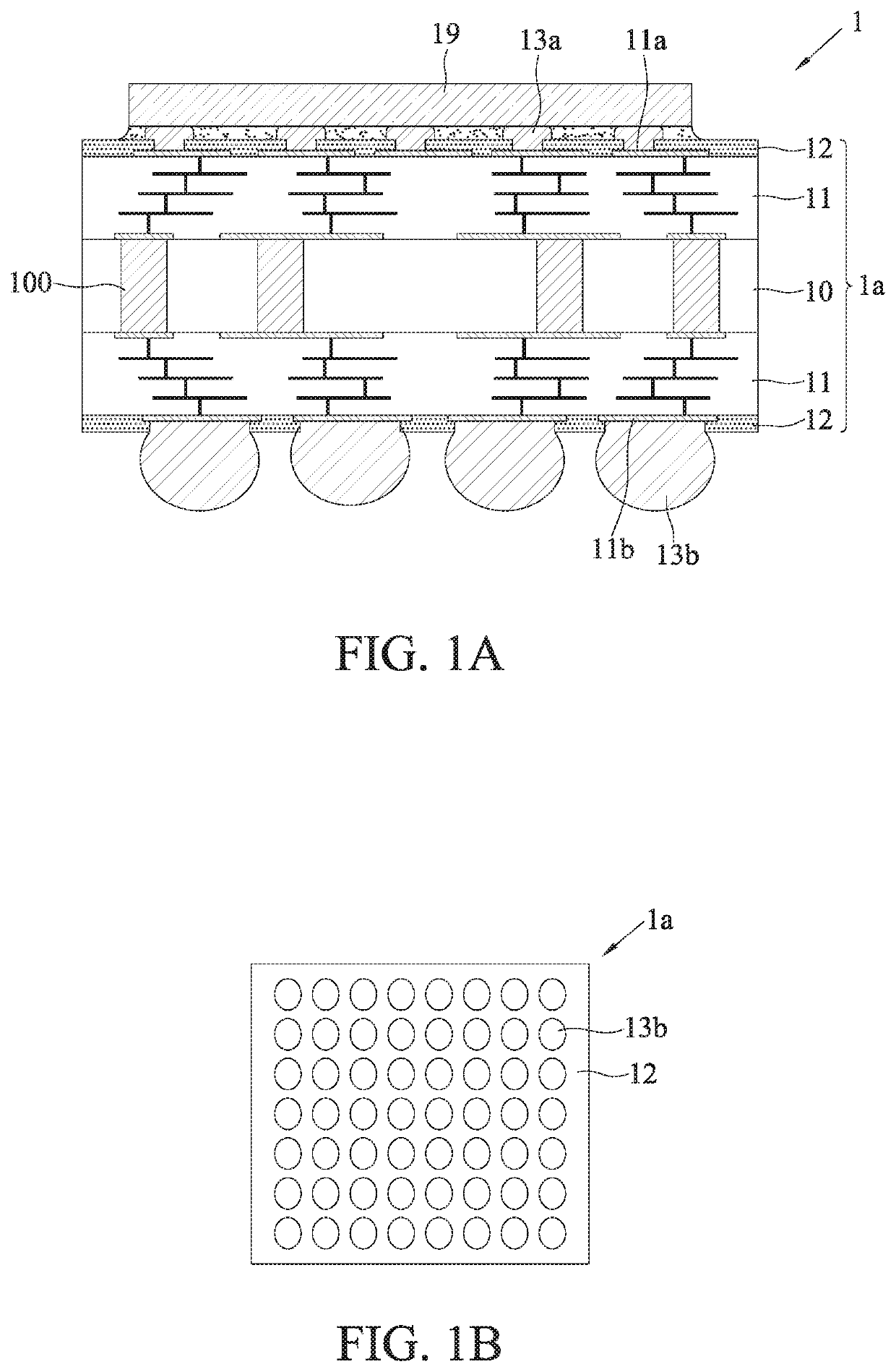
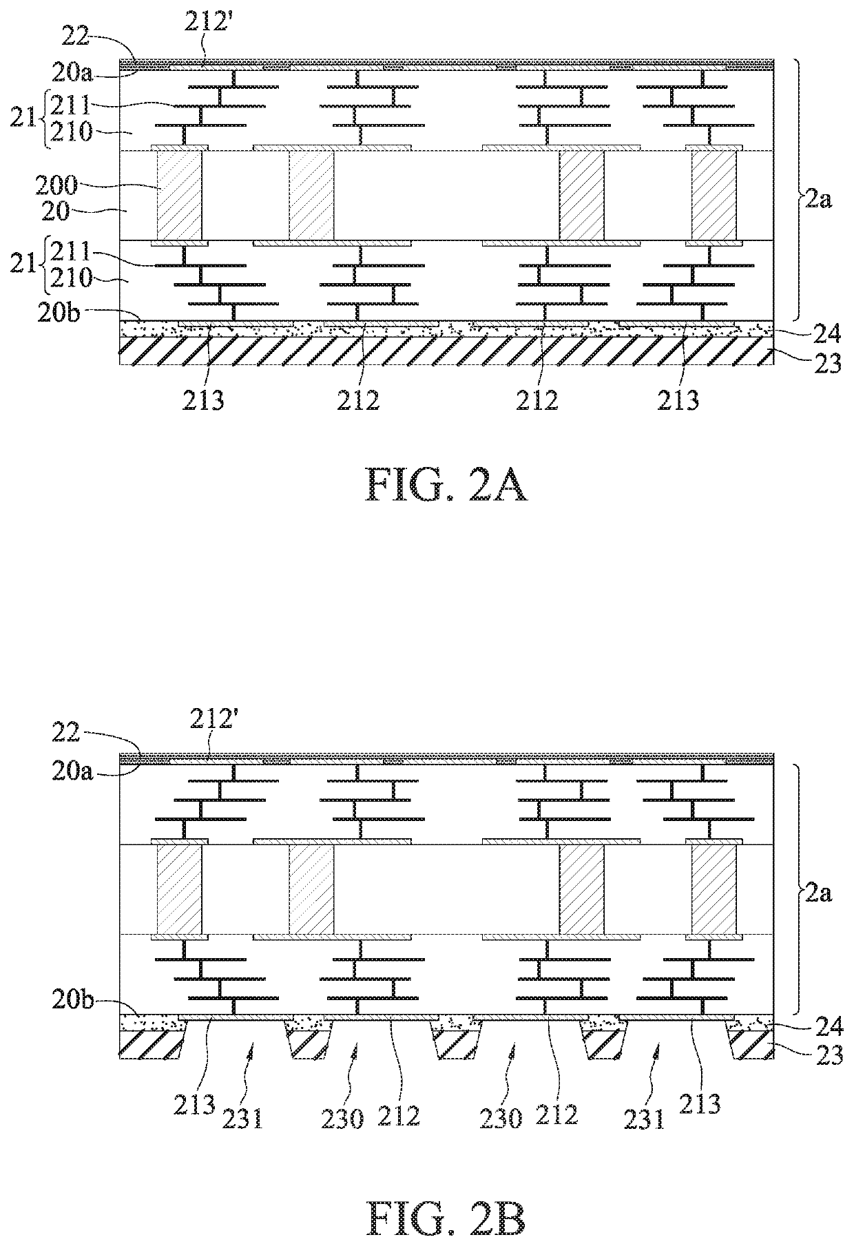
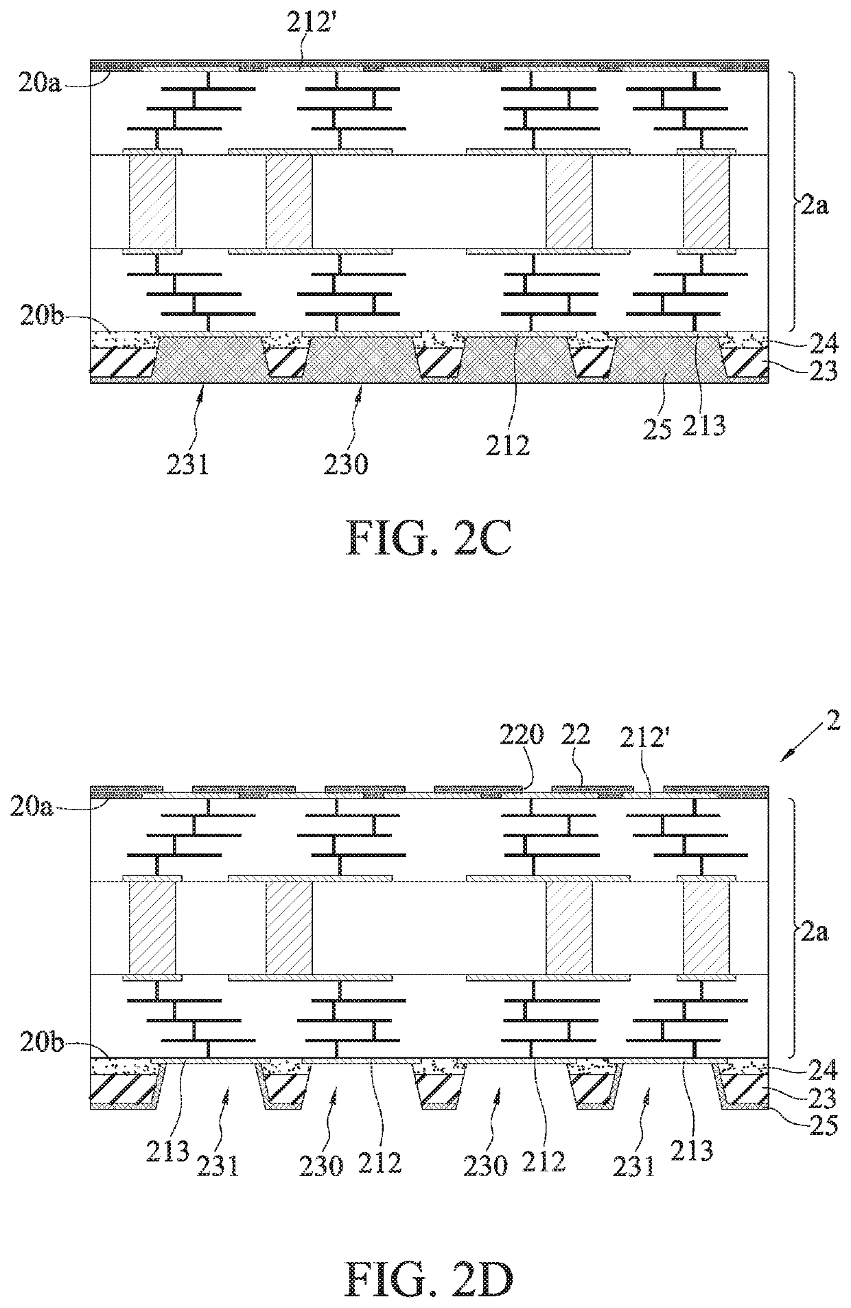
[0023]The following illustrative embodiments are provided to illustrate the present disclosure, these and other advantages and effects can be apparently understood by those in the art after reading the disclosure of this specification.

[0024]It should be appreciated that the structures, proportions, size and the like of the figures in the present disclosure are intended to be used in conjunction with the disclosure of the specification. They are not intended to limit the invention and therefore do not represent any substantial technical meanings. The details of the specification may be on the basis of different points and applications, and numerous modifications and variations can be devised without departing from the spirit of the present disclosure. As used herein, the terms “over,”“first,”“second,”“a” and the like, are used to distinguish one element from another, and are not intended to limit the scope of the present disclosure. Changes or adjustments are considered to be within ...


PUM

PropertyMeasurementUnit
electricallyaaaaaaaaaa
conductiveaaaaaaaaaa
sizeaaaaaaaaaa

Abstract

A semiconductor package substrate, a method for fabricating the same, and an electronic package having the same are provided. The method includes: providing a circuit structure having a first solder pad and a second solder pad; forming on the circuit structure a metal sheet having a first hole, from which the first solder pad is exposed, and a second hole, from which the second solder pad is exposed; and forming an insulation layer on the metal sheet and a hole wall of the second hole. A first conductive element that is to be grounded is disposed in the first hole and is in contact with the metal sheet and the first solder pad. Therefore, heat generated in a signal transmission process is dissipated by the metal sheet and the first conductive element.

Description

CROSS-REFERENCE TO RELATED APPLICATIONS[0001]This application claims priority to Taiwanese Application Serial No. 108119907, filed on Jun. 10, 2019. The entirety of the application is hereby incorporated by reference herein and made a part of this specification.BACKGROUND1. Technical Field[0002]The present disclosure relates to package substrates, and, more particularly, to a carrier substrate that can dissipate heat and an electronic package having the carrier substrate.2. Description of the Prior Art[0003]In recent years, more and more large size chips, such as artificial intelligence (AI) chips, advanced chips, or stacked chips have come to the market. Accordingly, sophisticated fabrication processes, such as 3D or 2.5D IC fabrication process, are developed and applied to advanced products, such as AI chips, GPU, etc., which require high density circuits / high transmission speed / high number of stacked layer / large size.[0004]Accordingly, fabricators use a large-sized flip-chip pack...

Claims


Application Information

Patent Timeline
Patent Type & Authority Patents(United States)
IPC IPC(8): H01L23/498H01L21/48H01L23/367H01L23/00
CPCH01L23/49838H01L21/4853H01L23/367H01L23/49816H01L24/73H01L2224/73204H01L23/498H01L23/49827H01L21/4846H01L21/486H01L23/31H01L2224/32225H01L2924/15311H01L23/49894H01L23/145H01L23/49822H01L2224/16237H01L24/16H01L2224/131H01L2224/16225H01L2924/00H01L2924/014H01L2924/00014
Inventor CHOU, PAO-HUNGYU, CHUN-HSIENHSU, SHIH-PING
Owner PHOENIX PIONEER TECH
Why Eureka
Try Eureka