

Selective deposition of solder ball contacts
a technology solder ball, which is applied in the direction of basic electric elements, electrical apparatus, semiconductor devices, etc., can solve the problems of increasing the number of input/output terminals required for the semiconductor die, increasing the complexity of the circuit, and increasing the number of solder ball contacts
- Summary
- Abstract
- Description
- Claims
- Application Information
AI Technical Summary
Problems solved by technology
Method used
Image

Examples
Embodiment Construction
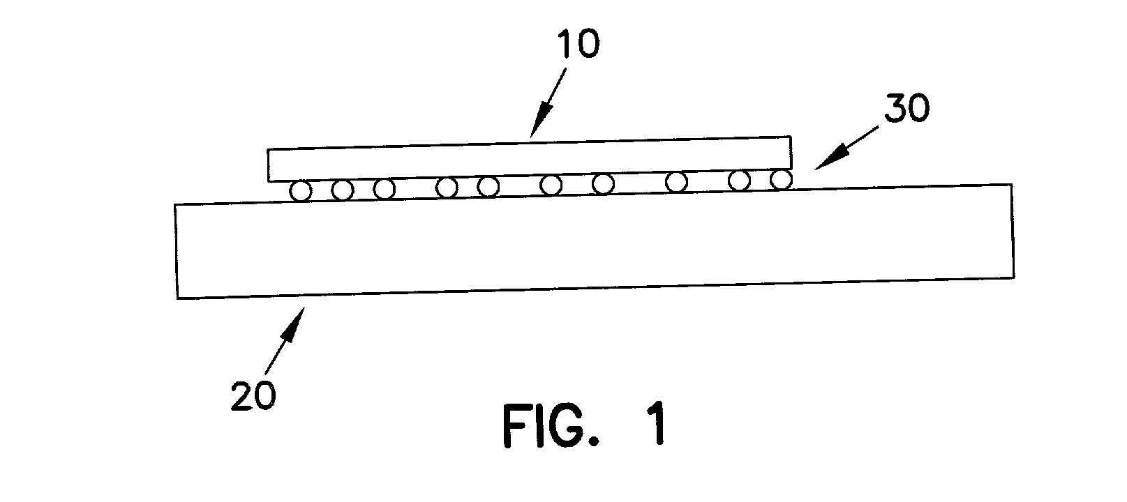
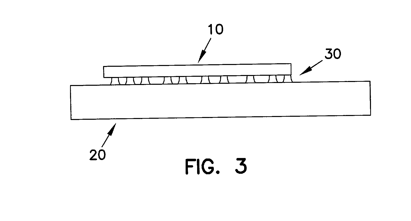
[0032] In the following detailed description, reference is made to the accompanying drawings which form a part hereof, and in which is shown by way of illustration specific embodiments in which the invention may be practiced. These embodiments are described in sufficient detail to enable those skilled in the art to practice the invention, and it is to be understood that other embodiments may be utilized and that structural, logical and electrical changes may be made without departing from the spirit and scope of the invention. The following detailed description is, therefore, not to be taken in a limiting sense, and the scope of the invention is defined by the appended claims. Like numbers in the figures refer to like components, which should be apparent from the context of use.
[0033] One embodiment of a process of the invention is explained below with reference to FIGS. 4(A)-4(P). Although the following explanation refers to a technique for placing solder ball contacts on a semicon...
PUM
 Abstract
Description
Claims
Application Information