Multi-layer circuit board with supporting layers of different materials
What is Al technical title?
Al technical title is built by PatSnap Al team. It summarizes the technical point description of the patent document.
a technology of supporting layers and circuit boards, applied in the direction of printed circuit manufacturing, dielectric characteristics, thermoplastic polymer dielectrics, etc., can solve the problems of increasing manufacturing costs, increasing the difficulty of producing circuit boards with small conducting patterns, and altering the shape of conducting patterns, etc., to achieve the effect of cheap and simple us
Inactive Publication Date: 2001-08-30
TELEFON AB LM ERICSSON (PUBL)
View PDF0 Cites 19 Cited by
Summary
Abstract
Description
Claims
Application Information
AI Technical Summary
This helps you quickly interpret patents by identifying the three key elements:
Problems solved by technology
Method used
Benefits of technology
[0010] The problem which is solved by the present invention is thus to achieve a method for manufacturing multi-layer circuit boards, which method is cheap and simple to use, and allows the various supporting layers in the board to be fastened in place without adhesive strata or other intermediate strata.
[0012] Starting from the first supporting layer, new supporting layers are arranged successively, in which, as material for each new supporting layer, a material is chosen with lower melting point than the supporting layer which is closest in the direction of the first supporting layer. Each new supporting layer is attached to the structure by exposing the structure to a temperature which exceeds the melting point of the new supporting layer but is lower than the melting point for the supporting layer which is closest in the direction of the first supporting layer. In this way, the conducting patterns present in the structure will not be affected by movements in their respective supporting layers.
Problems solved by technology
A problem which arises in this process is that when the supporting layers reach or exceed their melting point, the forms of the conducting patterns can alter due to movements in the supporting layers.
This adds to the difficulty of producing circuit boards with small conducting patterns and small intervals between the conducting patterns
This technique leads however to increased manufacturing costs, and results in the height of the structure becoming greater than desired.
A drawback with this method seems to be that each supporting stratum has to be surrounded by two other strata, whose only real function is that of adhesive layers.
This method appears to lead to higher material costs and multiple stages in the production of the circuit boards.
Method used
Image
Click on the blue label to locate the original text in one second.
Reading with bidirectional positioning of images and text.
Examples
Embodiment Construction
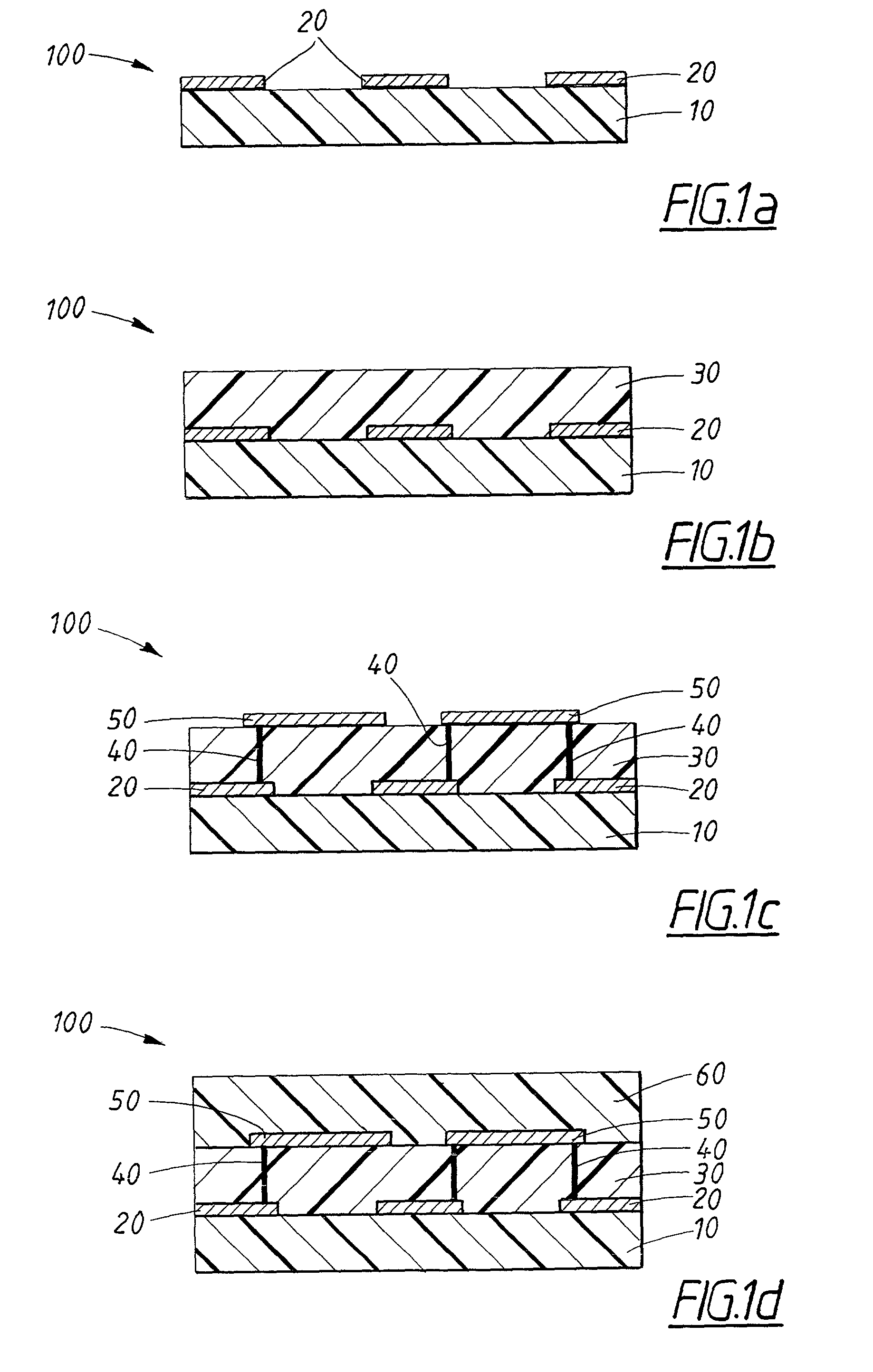
[0019] FIG. 1a illustrates in diagrammatic cross-section a supporting layer 10 bearing a conducting pattern 20. The supporting layer 10 will constitute a first layer in a structure 100 for a circuit board. The structure 100 will comprise a plurality of supporting layers for conducting patterns, which supporting layers are all of different materials.
[0020] A suitable material for the first layer 10 is a PTFE material (polytetrafluoroethylene) with a relatively large content of glass, thereby producing good dimensional stability, for example TACONIC TLC 32.RTM..
[0021] In FIG. 1b, the structure 100 from FIG. 1a is enlarged by a second supporting layer 30. As material for the second supporting layer 30, a material is chosen with lower melting point than the first supporting layer 10.
[0022] The second supporting layer 30 is attached to the structure 100 by exposing the structure 100, inclusive of the second supporting layer 30, to a temperature which exceeds the melting point for the sec...
PUM
Property
Measurement
Unit
melting points
aaaaa
aaaaa
melting points
aaaaa
aaaaa
melting points
aaaaa
aaaaa
Abstract
The invention relates to a press for manufacturing a structure (100) for a circuit board which comprises a plurality of supporting layers (10, 30, 60, 90), all of different materials, which supporting layers (10, 30, 60, 90) support electrically conducting patterns (20, 50, 70, 120). According to the process, the material for a first supporting layer (10) is that material which has the highest melting point of the different materials for supporting layers, subsequent to which, beginning from the first supporting layer (10), new supporting layers (30, 60, 90) are arranged successively. As material for each new supporting layer (30, 60, 90), a material is chosen with lower melting point than the supporting layer which is closest in the direction of the first supporting layer (10). Each new supporting layer (30, 60, 90) is attached to the structure (100) by exposing the structure (100) to a temperature which exceeds the melting point of the new supporting layer (30, 60, 90) but is lower than the melting point for that supporting layer which is the closest in the direction of the first supporting layer (10). Furthermore, on at least one side of each new supporting layer (30, 60, 90) electrically conducting patterns (50, 70, 120) are arranged, and the electrically conducting patterns (20, 50, 70, 120) on at least two supporting layers (10, 30, 60, 90) are connected to each other. The invention also relates to a circuit board manufactured according to this process.
Description
TECHNICAL FIELD[0001] The present invention relates to a process for manufacturing a multi-layer circuit board and a multi-layer circuit board manufactured according to this process.PRIOR ART[0002] A conventional technique for obtaining circuit boards with small interspaces between the components which are mounted on the surface of the circuit board, in other words circuit boards having a high so-called packing density, is to produce the circuit board as a multi-layer board. A multi-layer circuit board comprises a plurality of supporting layers of non-conducting material on which a conducting pattern is arranged. The conducting patterns on the various supporting layers are connected to one another in desired fashion through the creation of holes, so called "via-holes" , between the various supporting layers at the locations in which connection is required. The via-holes are made electrically conducting by being wholly or partially filled with electrically conducting material.[0003] ...
Claims
Application Information
Patent Timeline
Application Date:The date an application was filed.
Publication Date:The date a patent or application was officially published.
First Publication Date:The earliest publication date of a patent with the same application number.
Issue Date:Publication date of the patent grant document.
PCT Entry Date:The Entry date of PCT National Phase.
Estimated Expiry Date:The statutory expiry date of a patent right according to the Patent Law, and it is the longest term of protection that the patent right can achieve without the termination of the patent right due to other reasons(Term extension factor has been taken into account ).
Invalid Date:Actual expiry date is based on effective date or publication date of legal transaction data of invalid patent.
Patent Type & Authority Applications(United States)