Multi-master multi-slave system bus in a field programmable gate array (FPGA)

a gate array and multi-master technology, applied in the field of field programmable gate arrays (fpgas), can solve the problems of slow implementation and inefficient operation

Inactive Publication Date: 2002-01-24
LATTICE SEMICON CORP
View PDF0 Cites 26 Cited by
  • Summary
  • Abstract
  • Description
  • Claims
  • Application Information

AI Technical Summary

Problems solved by technology

However, conventional FPGA configuration logic is not available for access or use by FPGA components after configuration, leading to inefficient and slow implementations.

Method used


Image

  • Multi-master multi-slave system bus in a field programmable gate array (FPGA)
  • Multi-master multi-slave system bus in a field programmable gate array (FPGA)
  • Multi-master multi-slave system bus in a field programmable gate array (FPGA)

Examples


Embodiment Construction

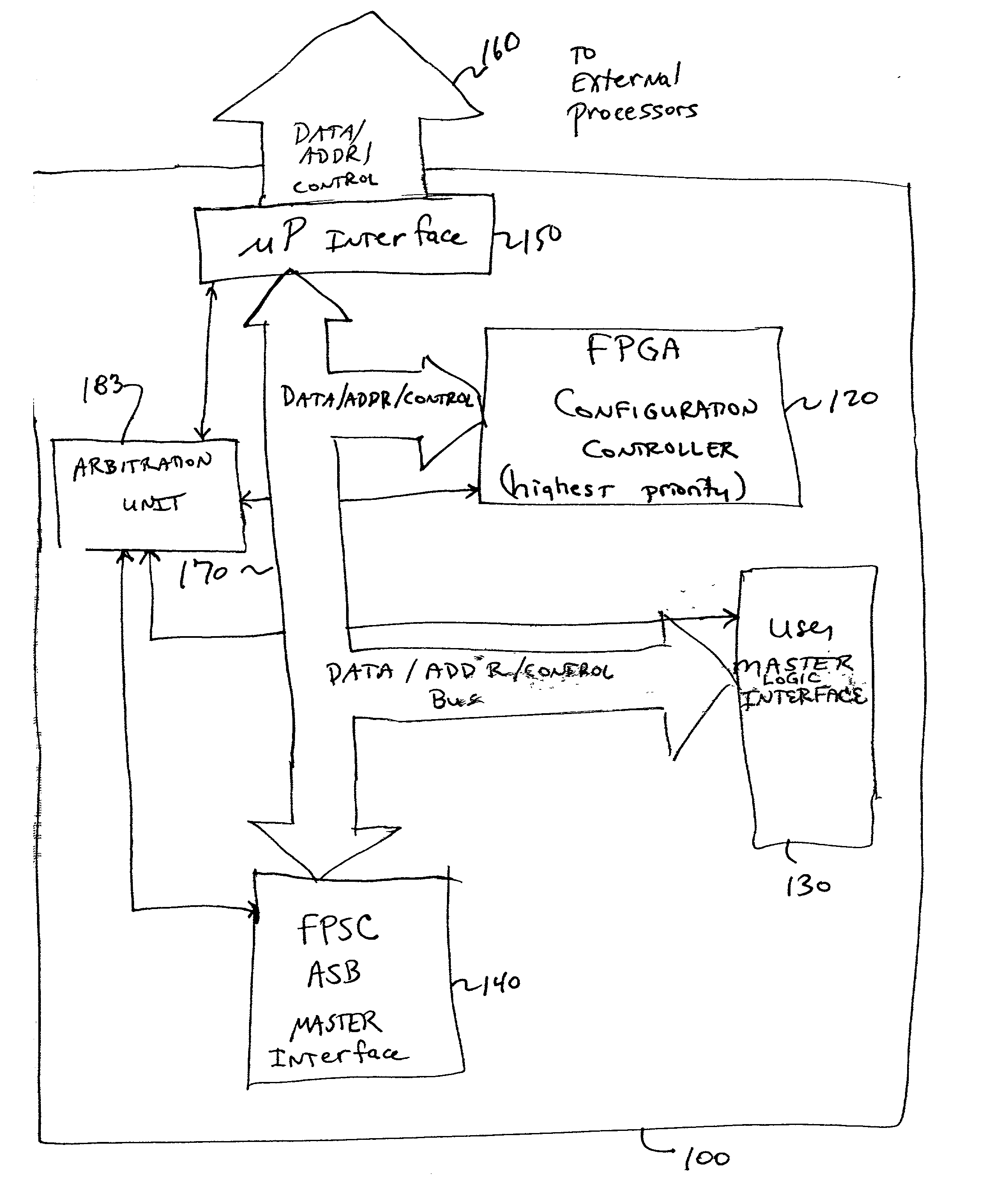
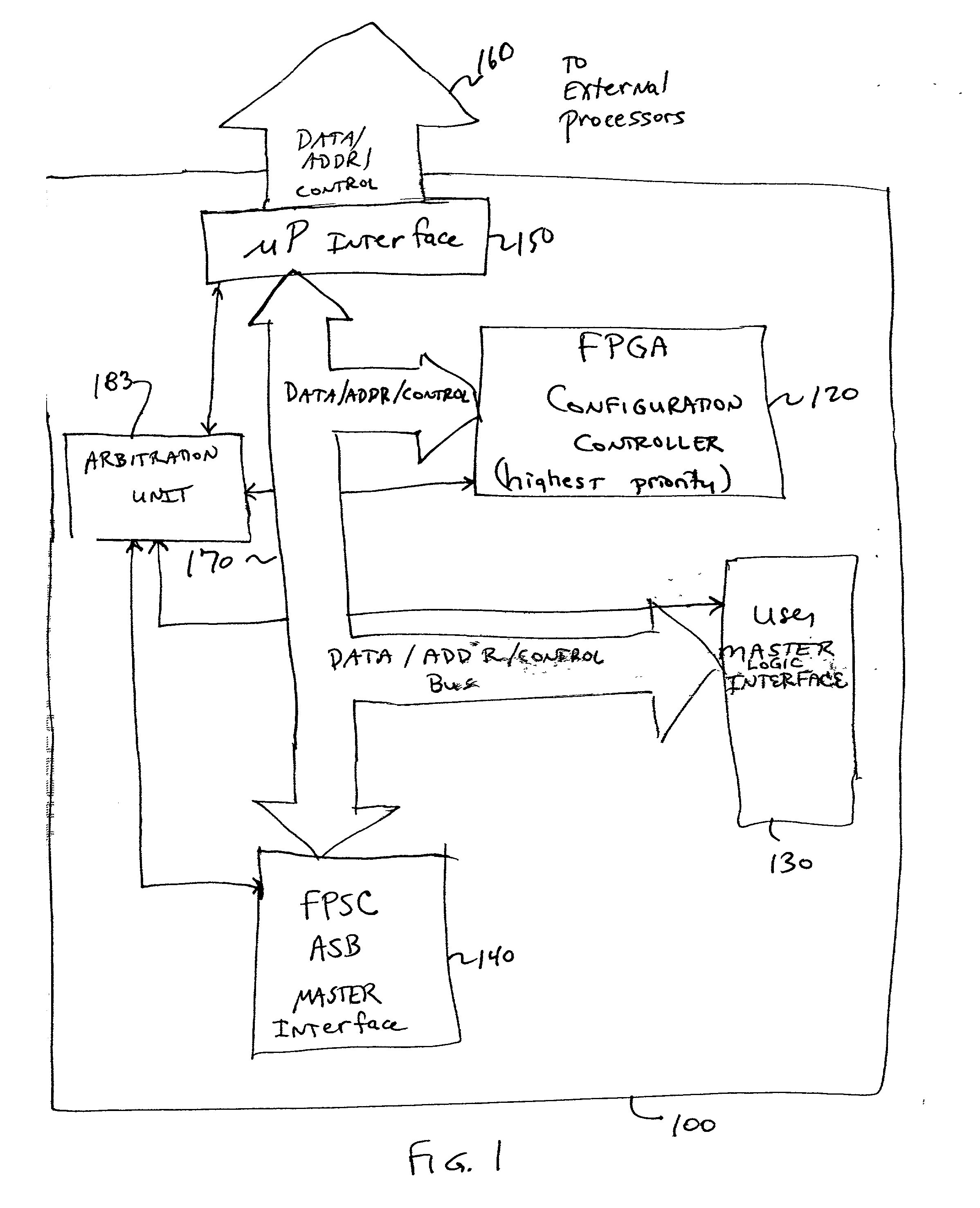
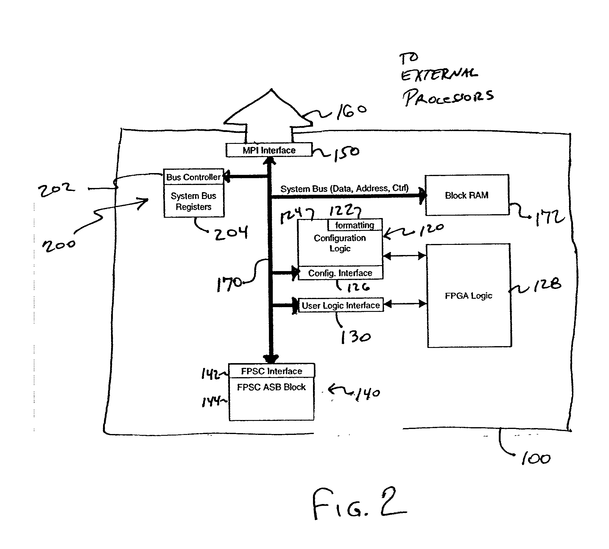
[0028] Conventional Field Programmable Gate Array (FPGA) devices provide external access to a single internal (i.e., embedded) element, i.e., the configuration memory. Conventional FPGA devices do not include an embedded system bus providing data, address and control between the external device and any embedded element other than the configuration memory.

[0029] In the disclosed embodiment, a SRAM based FPGA includes a hierarchical architecture of logic, clocks, routing, RAM, and system-level blocks creating a seamless merge of FPGA and ASIC designs.

[0030] The FPGA architecture comprises four basic elements: programmable logic cells (PLCs), programmable I / O cells (PIOs), embedded block RAMs (EBRs), and system-level features, interconnected with both global and local wires.

[0031] An array of PLCs are surrounded by common interface blocks which provide an abundant interface to the adjacent PLCs or system blocks. Each PLC may contain, e.g., a PFU, a SLIC, local routing resources, and co...


PUM


Abstract

An embedded system bus is woven between a plurality of embedded master elements and at least one slave element within the FPGA device, and provides an external processor interface allowing direct access to any of the plurality of embedded slave elements. Using the embedded system bus, any of a plurality of masters may be allowed to program an embedded element, e.g., embedded FPGA logic, whereas conventional FPGAs allowed only a single master (e.g., a processor) to program the embedded FPGA logic. The embedded system bus is a group of signals, typically data, address and control, that connects system elements together and provides a basic protocol for the flow of data. The embedded system bus allows for control, configuration and status determination of the FPGA device. The embedded system bus is preferably a dedicated function available at all times for arbitrated access to allow communication between the various embedded system components.

Description

[0001] This application claims priority from U.S. Provisional Application No. 60 / 207,371 entitled "Novel Field Programmable Gate Array" filed on May 26, 2000, the specification of which is hereby expressly incorporated herein by reference.[0002] 1. Field of the Invention[0003] This invention relates generally to field programmable gate arrays (FPGAs). In particular, it relates to the implementation of improved architectures and functions within an FPGA.[0004] 2. Background of Related Art[0005] A Field Programmable Gate Array (FPGA) is a programmable integrated circuit which provides a customized logic array and functionality to a particular customer.[0006] FIG. 4 depicts a conventional Field Programmable Gate Array (FPGA).[0007] In particular, as shown in FIG. 4, an FPGA 400 typically includes four distinct features: configuration memory 406, input / output (I / O) blocks 408-414, configurable logic blocks 404, and a routing network 402 between the internal components.[0008] Configurati...

Claims


Application Information

Patent Timeline
Patent Type & Authority Applications(United States)
IPC IPC(8): G06F1/10G06F13/36G06F13/20H01L21/82H01L21/822H01L27/04H03K5/13H03K19/0175H03K19/173H03K19/177H03L7/081H03L7/099
CPCG06F1/10H03K5/13H03K19/017581H03K19/17732H03K19/17736H03K19/1774H03K5/133H03K19/17748H03K19/1776H03K19/17788H03K19/17792H03L7/081H03L7/0996H03K19/17744
Inventor BRITTON, BARRY K.CHARATH, RAVIKUMARCHEN, ZHENGHOFF, JAMES F.LANSENDERFER, CORT D.MCCARLEY, DON
Owner LATTICE SEMICON CORP
Why Eureka
Try Eureka