
Integrated circuits protected against reverse engineering and method for fabricating the same using etched passivation openings in integrated circuits

a technology of integrated circuits and reverse engineering, which is applied in the direction of electrical equipment, semiconductor devices, semiconductor/solid-state device details, etc., can solve the problems of reverse engineering not being able to help in destroying important parts of the circuit, destruction of important elements and data

Inactive Publication Date: 2002-07-25
HRL LAB
View PDF0 Cites 29 Cited by
  • Summary
  • Abstract
  • Description
  • Claims
  • Application Information

AI Technical Summary

Benefits of technology

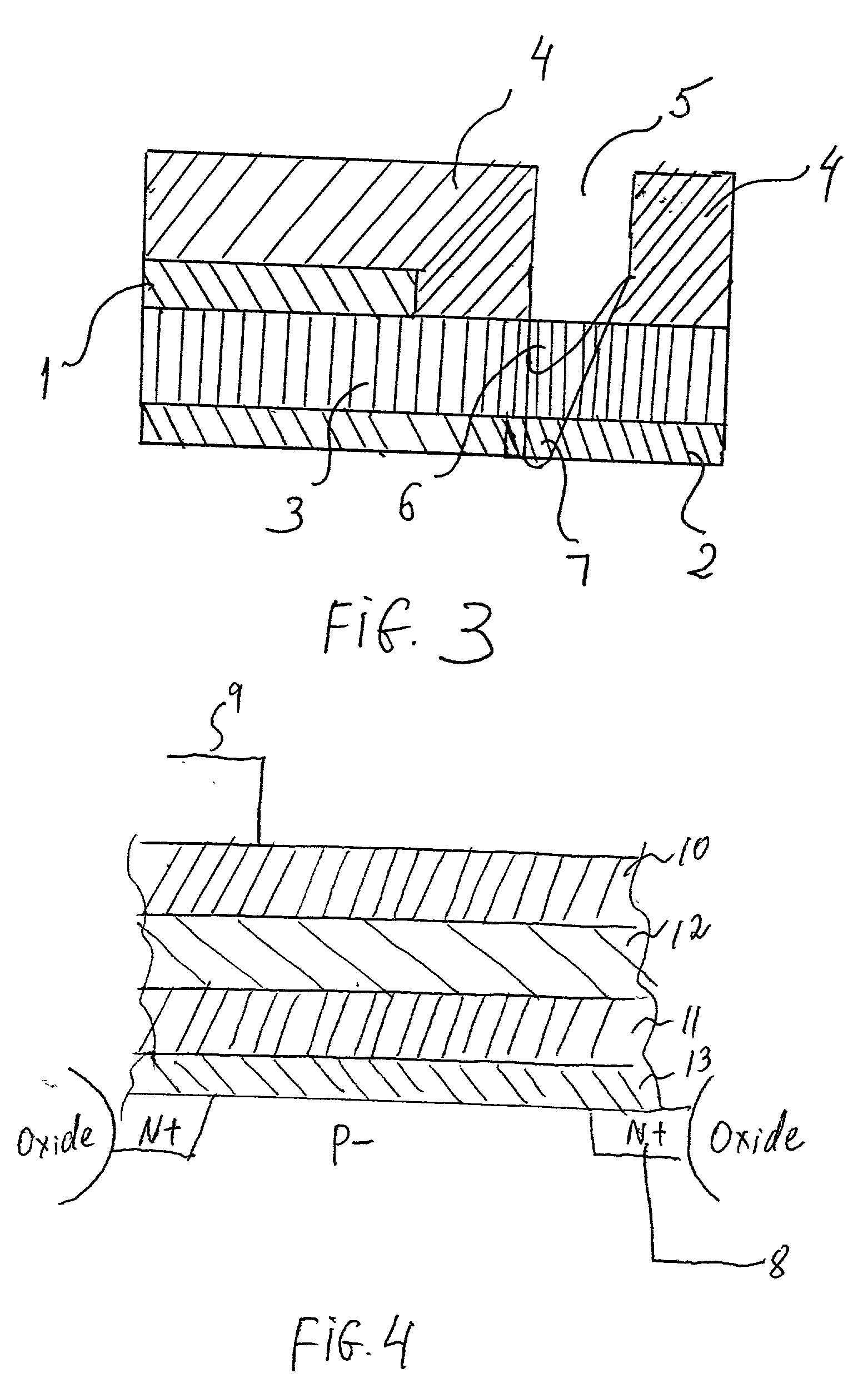
[0017] The gist of this invention is to provide an extra opening in the passivation layer, for example, an opening that is not required for a contact metal. In this case, normal, careful deprocessing by the reverse engineer will lead to the destruction of important elements and data because of the deeper etching that will occur in the region of the passivation opening. In other words, in order to learn the design of the integrated circuit, the reverse engineer cannot help destroying important portions of the circuit. This kind of protection will substantially assist in protecting the integrated circuit against reverse engineering.

Problems solved by technology

In this case, normal, careful deprocessing by the reverse engineer will lead to the destruction of important elements and data because of the deeper etching that will occur in the region of the passivation opening.
In other words, in order to learn the design of the integrated circuit, the reverse engineer cannot help destroying important portions of the circuit.

Method used


Image

  • Integrated circuits protected against reverse engineering and method for fabricating the same using etched passivation openings in integrated circuits
  • Integrated circuits protected against reverse engineering and method for fabricating the same using etched passivation openings in integrated circuits
  • Integrated circuits protected against reverse engineering and method for fabricating the same using etched passivation openings in integrated circuits

Examples


Embodiment Construction

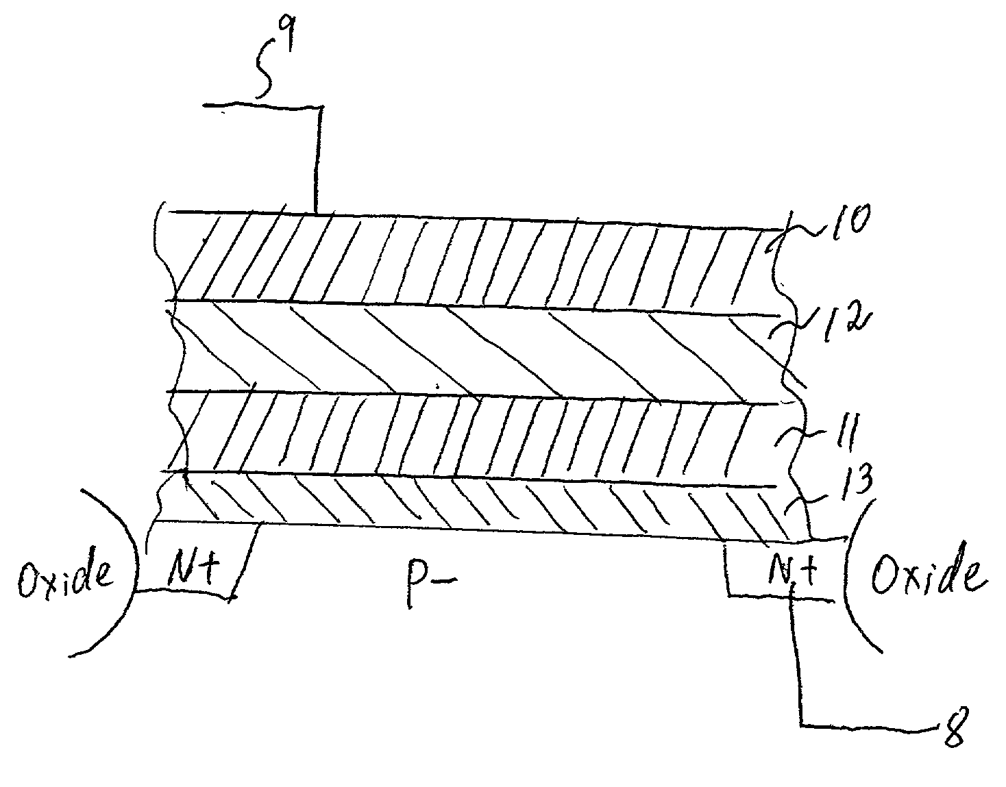
[0025] This invention can be used on any semiconducting device, including CMOS, bipolar silicon or group III-group V integrated circuits.

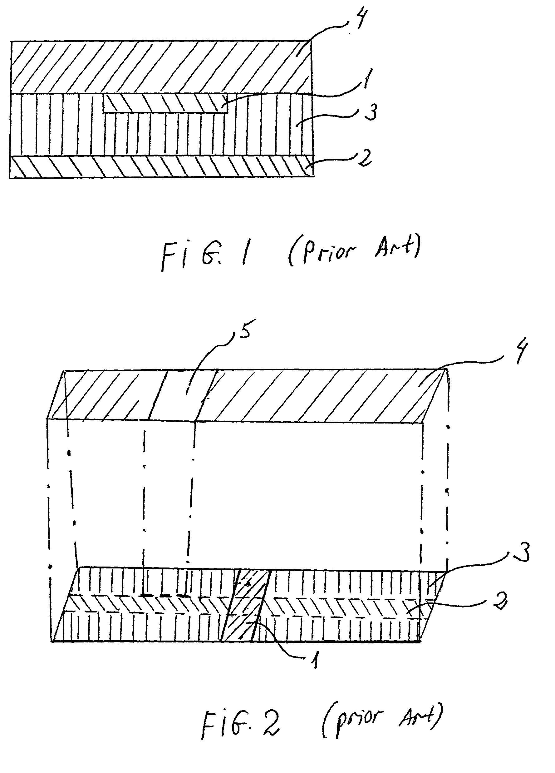
[0026] FIG. 1 shows a typical cross-section view of a part of a device comprising a plurality of metal layers. Top metal layer 1 and a next metal layer 2 are separated by an insulating layer 3, preferably, a silicon oxide layer. Each metal layer 1 and 2 has a preferable thickness of about 200 Angstroms, and the insulating layer 3 has a thickness preferably within a range of between 3,000 Angstroms and 5,000 Angstroms. The insulating layer 3 is disposed on a semiconducting substrate, such as that used in integrated circuits (not shown). Only two metal layers 1 and 2 are shown on FIGS. 1-3 for the purposes of illustration of the inventive concept; however, it should be understood that more than two metal layers are typically present and indeed many other metal layers may be present.

[0027] A passivation layer 4, preferably an oxide, a nitride or a pol...


PUM


Abstract

Semiconducting devices, including integrated circuits, protected from reverse engineering comprising passivation openings made in a passivation layer. When a reverse engineer etches away the passivation layer, underlying metal layers and / or other elements of the device are destroyed making the reverse engineering impossible. Top metal layer may remain intact. A method for fabricating such devices.

Description

I. BACKGROUND OF THE INVENTION[0001] 1. Field of the Invention[0002] This invention relates to the field of the prevention of reverse engineering of integrated circuits and / or making such reverse engineering so difficult and time-consuming as to make reverse engineering of integrated circuits non-feasible.[0003] More particularly, this invention relates to using, in order to prevent and / or discourage such reverse engineering, openings etched in the passivation layer, typically, the uppermost insulating layer disposed atop an integrated circuit.[0004] 2. Description of the Related Art[0005] The design and development of semiconductor integrated circuits require a thorough understanding of the complex structures and processes and involve many man-hours of work requiring high skill, costing considerable sums of money.[0006] In order to avoid these expenses, some developers stoop to the contentious practice of reverse engineering, disassembling existing devices manufactured by somebody ...

Claims


Application Information

Patent Timeline
Patent Type & Authority Applications(United States)
IPC IPC(8): H01L23/58
CPCH01L23/57H01L2924/0002H01L2924/00
Inventor CHOW, LAP-WAIBAUKUS, JAMES P.CLARK, WILLIAM M. JR.
Owner HRL LAB
Learn More