Method for test optimization using historical and actual fabrication test data

a technology of historical and actual fabrication and test data, applied in the direction of individual semiconductor device testing, semiconductor/solid-state device testing/measurement, instruments, etc., can solve the problems of inconsistency of tests, increased cost per yield, and current methods that include manual pattern ordering that does not provide real-time testing

Inactive Publication Date: 2002-10-24
CADENCE DESIGN SYST INC
View PDF5 Cites 57 Cited by
  • Summary
  • Abstract
  • Description
  • Claims
  • Application Information

AI Technical Summary

Problems solved by technology

As the complexity of the semiconductor devices increases, conventional testing methods of integrated circuit (IC) wafers during production involve comprehensive testing methods that greatly require longer time periods to yield useful updated results for production controls resulting in greater cost per yield.
Empirical data consistently shows that a relatively small number of tests typically detect all the failures

Method used


Image

  • Method for test optimization using historical and actual fabrication test data
  • Method for test optimization using historical and actual fabrication test data
  • Method for test optimization using historical and actual fabrication test data

Examples


Embodiment Construction

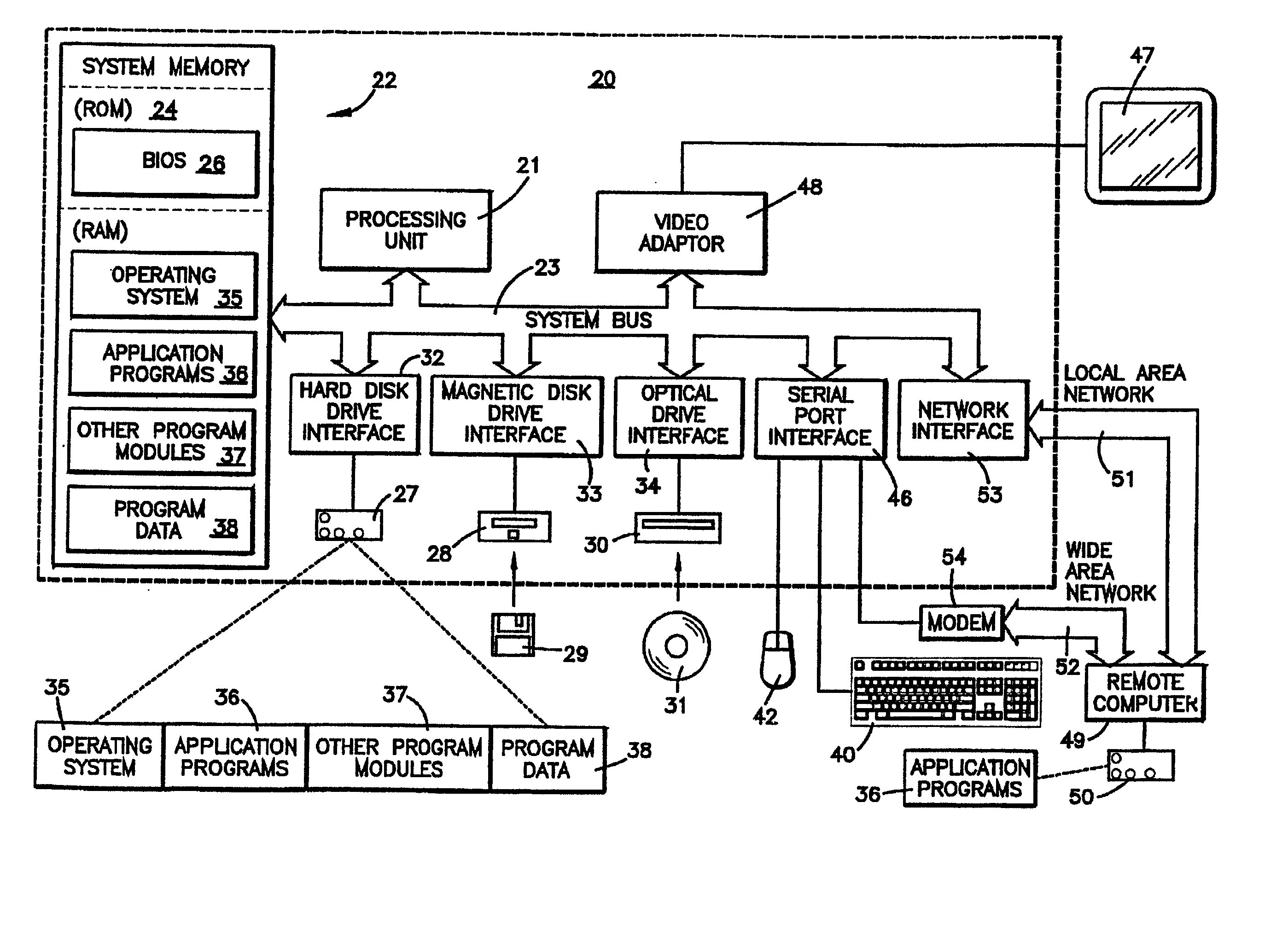
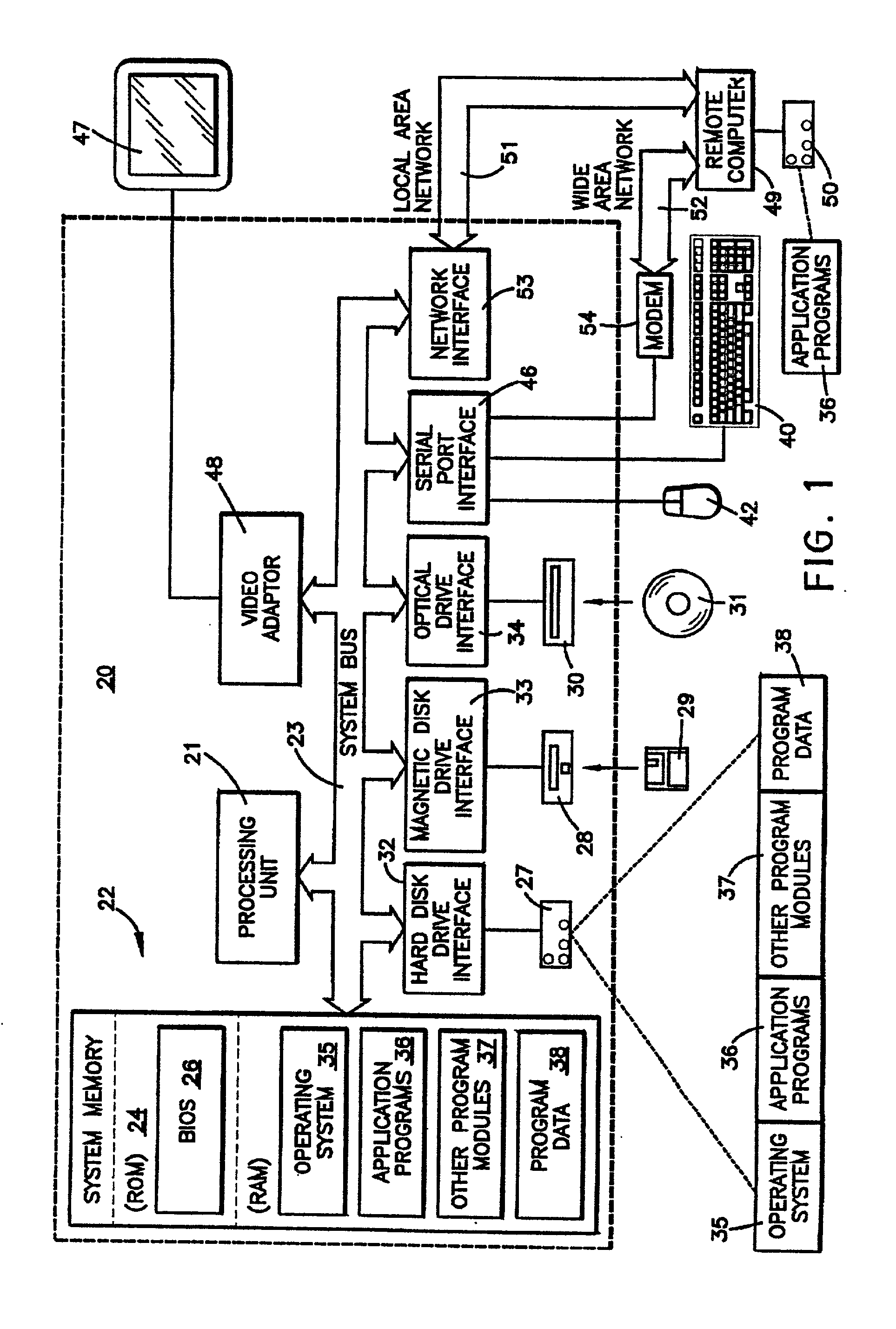
[0012] The present invention is primarily disclosed as a method, it will be understood by a person of ordinary skill in the art that an apparatus, such as a conventional data processor, including a CPU, memory, I / O, program storage, a connecting bus, and other appropriate components, could be programmed or otherwise designed to facilitate the practice of the method of the invention. Such a processor would include appropriate program means for executing the method of the invention. Also, an article of manufacture, such as a pre-recorded disk or other similar computer program product, for use with a data processing system, could include a storage medium and program means recorded thereon for directing the data processing system to facilitate the practice of the method of the invention. It will be understood that such apparatus and articles of manufacture also fall within the spirit and scope of the invention.

[0013] FIG. 1 shows an exemplary data processing system for practicing the me...


PUM


Abstract

A method and system are provided that minimize wafer or package level test time without adversely impacting yields in downstream manufacturing processes or degrading outgoing quality levels. The method provides optimization by determining, a priority, the most effective set of tests for a given lot or wafer. The invention implements a method using a processor-based system involving the integration of multiple sources of data that include: historical and realtime, product specific and lot specific, from wafer fabrication data (i.e., process measurements, defect inspections, and parametric testing), product qualification test results, physical failure analysis results and manufacturing functional test results. These various forms of data are used to determine an optimal set of tests to run using a test application sequence, on a given product to optimize test time with minimum risk to yield or product quality.

Description

[0001] 1. Field of the Invention[0002] The present invention generally relates to a system and method for adaptive optimization of a testing procedure for integrated circuits being made with given quality control level(s).[0003] 2. Description of the Related Art[0004] As the complexity of the semiconductor devices increases, conventional testing methods of integrated circuit (IC) wafers during production involve comprehensive testing methods that greatly require longer time periods to yield useful updated results for production controls resulting in greater cost per yield. Empirical data consistently shows that a relatively small number of tests typically detect all the failures on any given lot of wafer production, but that these tests are not necessarily consistent from lot to lot, or sometimes even wafer to wafer. Furthermore, current methods include manual pattern ordering that does not provide real-time testing based on a set of comprehensive inputs that include current yield r...

Claims


Application Information

Patent Timeline
IPC IPC(8): H01L21/66
CPCH01L22/20
Inventor BULAGA, RAYMOND J.GATTIKER, ANNE E.HARRIS, JOHN L.NIGH, PHILLIP J.NOEL, LEO A.THIBAULT, WILLIAM J.VAN HORN, JODY J.WHEATER, DONALD L.
Owner CADENCE DESIGN SYST INC
Why Eureka
Try Eureka