Instruction processing method for verifying basic instruction arrangement in VLIW instruction for variable length VLIW processor

Inactive Publication Date: 2002-10-31
FUJITSU LTD
View PDF22 Cites 24 Cited by
  • Summary
  • Abstract
  • Description
  • Claims
  • Application Information

AI Technical Summary

Problems solved by technology

It should be noted, however, that making a different language processing system w

Method used


Image

  • Instruction processing method for verifying basic instruction arrangement in VLIW instruction for variable length VLIW processor
  • Instruction processing method for verifying basic instruction arrangement in VLIW instruction for variable length VLIW processor
  • Instruction processing method for verifying basic instruction arrangement in VLIW instruction for variable length VLIW processor

Examples


first embodiment

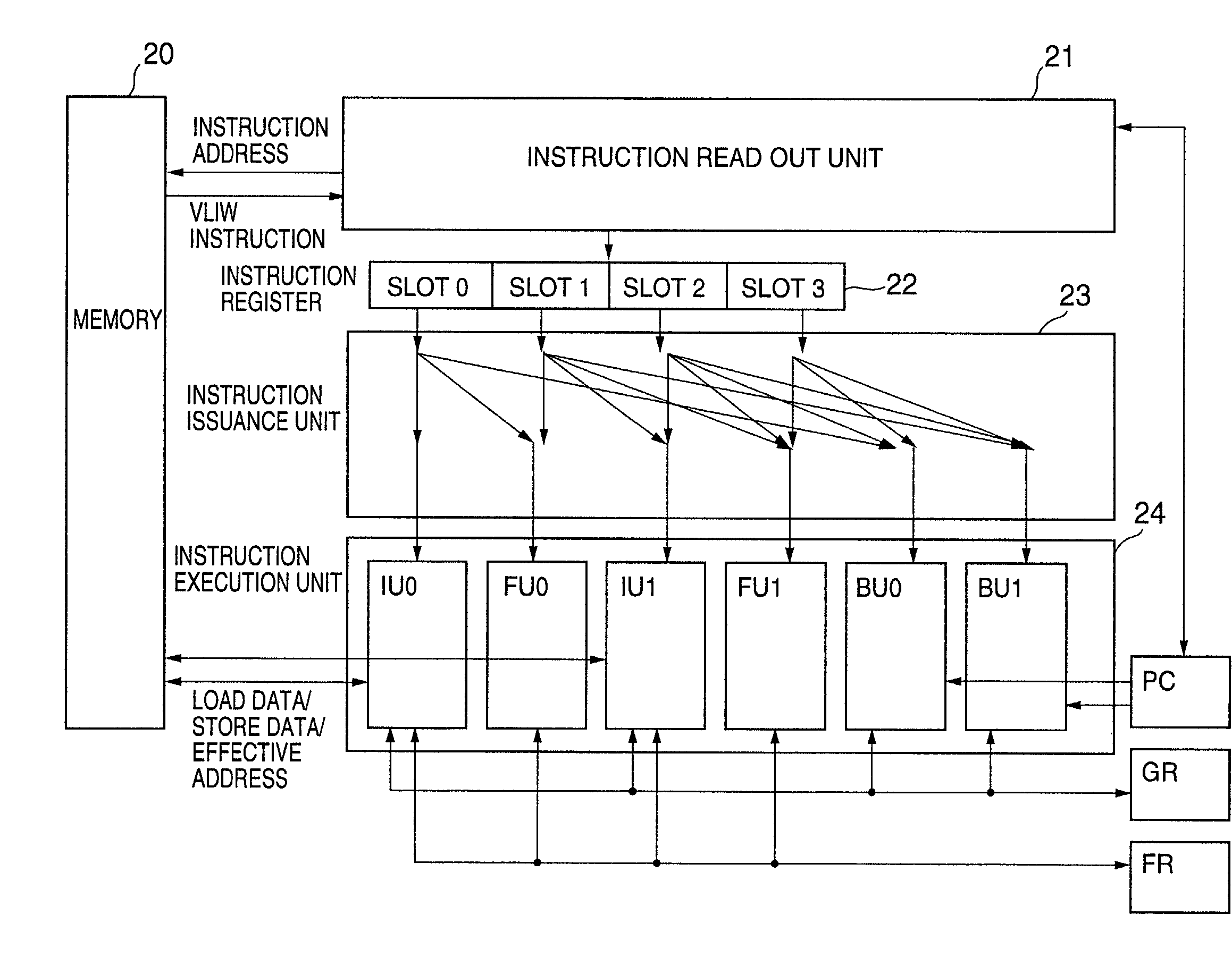
[0111] FIG. 10 is a block diagram of a variable length VLIW processor which can execute at most 4 instructions at a time. This processor includes a memory 20, an instruction readout unit 21, an instruction register 22, an instruction issuance unit 23, and an instruction execution unit 24. The instruction execution unit 24 includes integer units IU0 and IU1, floating point units FU0 and FU1, and branch units BU0 and BU1. This processor further includes a general purpose register GR, a floating point register FR, and a program counter PC.

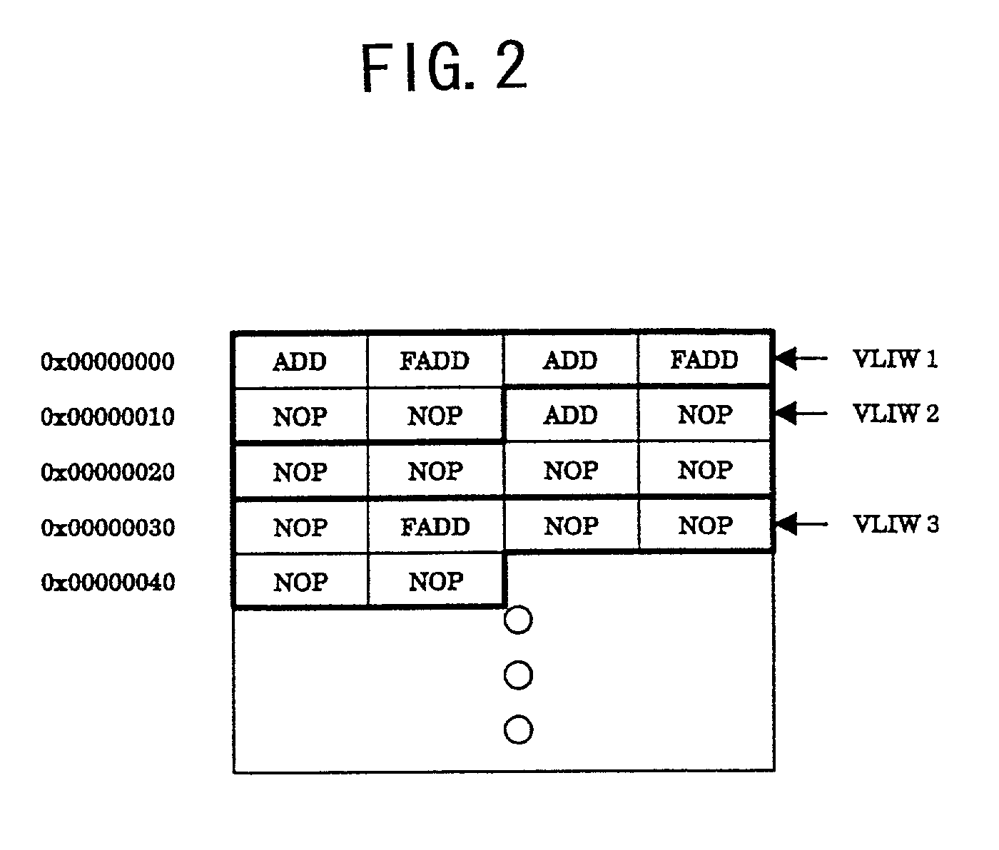
[0112] It is assumed in this description that 22 sets of basic instructions listed in FIG. 11 are allowed as an arrangement of a VLIW instruction. Symbols used in FIG. 11 have the following meanings. I0 means that an executable basic instruction is provided to IU0. I1 means that an executable basic instruction is provided to IU1. F0 means an executable basic instruction is provided to FU0. F1 means that an executable basic instruction is provided to F...

second embodiment

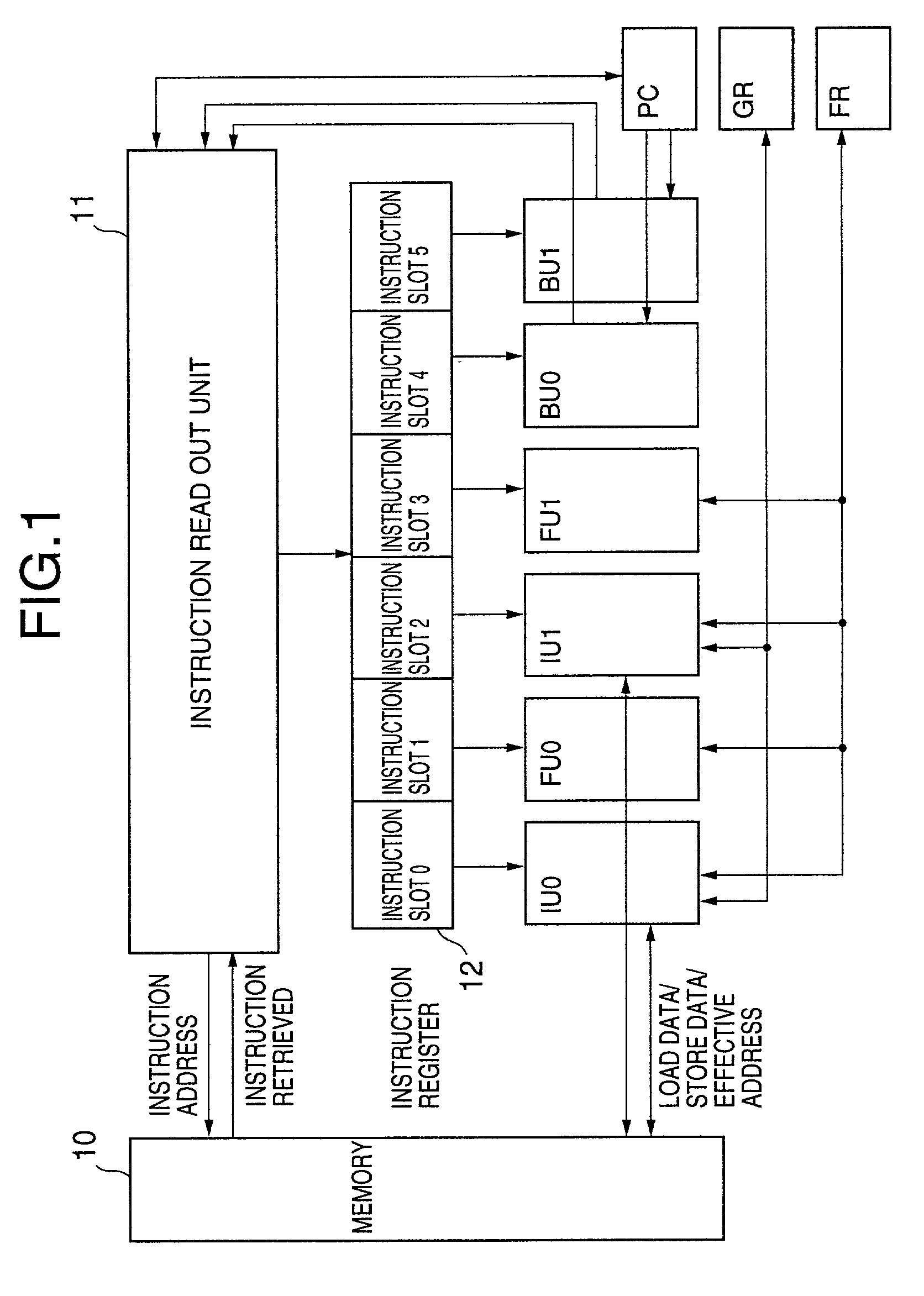
[0197] FIG. 31 shows a variable length VLIW processor which can execute at most 8 instructions at the same time. It will be assumed in the following description that basic instruction arrangements are checked by applying the first basic instruction arrangement verification algorithm previously described in relation to an assembler.

[0198] The variable length VLIW processor shown in FIG. 31 includes a memory 120, an instruction readout unit 121, an instruction register 122, an instruction issuance unit 123, an instruction execution unit 124, a general purpose register GR, a floating register FR, and a program counter PC. The instruction execution unit 124 includes integer units IU0, IU1, IU2, and IU3, and floating units FU0, FU1, FU2, and FU3, and branch units BU0, BU1, BU2, and BU3.

[0199] As shown in FIG. 32 and FIG. 33, it is assumed that 73 basic instruction arrangements in a VLIW instruction are executable with this processor.

[0200] The instruction readout unit 121 retrieves from ...

third embodiment

[0214] In the third embodiment, a basic instruction arrangement in a VLIW instruction is verified by applying the second basic instruction arrangement verification algorithm to the variable length VLIW processor which can execute at most 4 basic instructions at the same time.

[0215] A processor is assumed to have the same structure as that of the first embodiment. The second basic instruction arrangement verification algorithm shown in FIG. 28 is used as the algorithm of the basic instruction verification unit 13A-1.

[0216] FIG. 38 is an instruction classification table used for the third embodiment. FIG. 39 is an instruction category table for the third embodiment. FIG. 40 is an instruction slot table for the third embodiment.

[0217]


PUM


Abstract

An instruction processing method for checking an arrangement of basic instructions in a very long instruction word (VLIW) instruction, suitable for language processing systems, an assembler and a compiler, used for processors which execute variable length VLIW instructions designed based on variable length VLIW architecture.

Description

[0001] 1. Field of the Invention[0002] Recent improvements in processing capacity of computer systems are mainly realized by improvement in processing capacity of processors, Central Processing Units (CPUs). The processing capacity of the processors is improved by increasing Instruction Level Parallelism (ILP), for example. Technologies such as Super-Scalar Architecture and Very Long Instruction Word Architecture (VLIW) are known as a method to increase the ILP.[0003] Various microprocessors are provided in electronic devices such as cellular phones, printers, and digital televisions. Those devices are called as Embedded Application device, and those microprocessors are called as Embedded Processors.[0004] Recent demands for high-performance embedded application devices require performance of embedded processors to be improved year by year. Some of the embedded processors have been improving their performance by increasing ILP.[0005] In a development of an embedded application devic...

Claims


Application Information

Patent Timeline
IPC IPC(8): G06F9/30G06F9/38G06F9/45
CPCG06F9/3885G06F8/447G06F9/38
Inventor KAMIGATA, TERUHIKOMIYAKE, HIDEO
Owner FUJITSU LTD
Why Eureka
Try Eureka