Centrifuge and method for centrifuging a semiconductor wafer

a technology of centrifugation and semiconductor wafer, which is applied in the direction of cleaning with liquids, lighting and heating apparatus, and separation processes, etc., can solve the problems the risk of semiconductor wafer contamination, and the possibility of uneven treatment of the rear sid

Inactive Publication Date: 2002-11-21
SILTRONIC AG
View PDF0 Cites 2 Cited by
  • Summary
  • Abstract
  • Description
  • Claims
  • Application Information

AI Technical Summary

Problems solved by technology

When using such a centrifuge, there is a risk of the semiconductor wafer being contaminated during centrifuging, for example by particles which emanate from the centrifuge.
Rebounding of drops which have been centrifuged off onto dry points on the semiconductor wafer may also lead to recontamination.
This rules out the possibility of uneven treatment of the rear side, as well as of periodic interruption of the supply

Method used


Image

  • Centrifuge and method for centrifuging a semiconductor wafer
  • Centrifuge and method for centrifuging a semiconductor wafer
  • Centrifuge and method for centrifuging a semiconductor wafer

Examples


Embodiment Construction

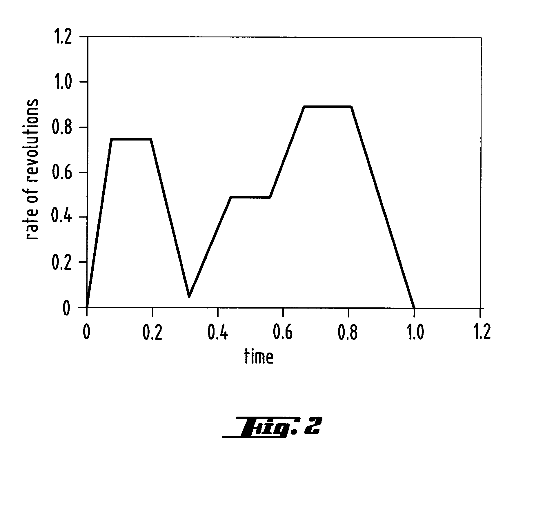
[0027] The following example is directed to a preferred embodiment of the method which refers to FIG. 2 which depicts the rotational speed of the centrifuge as a function of time. The method comprises the following steps:

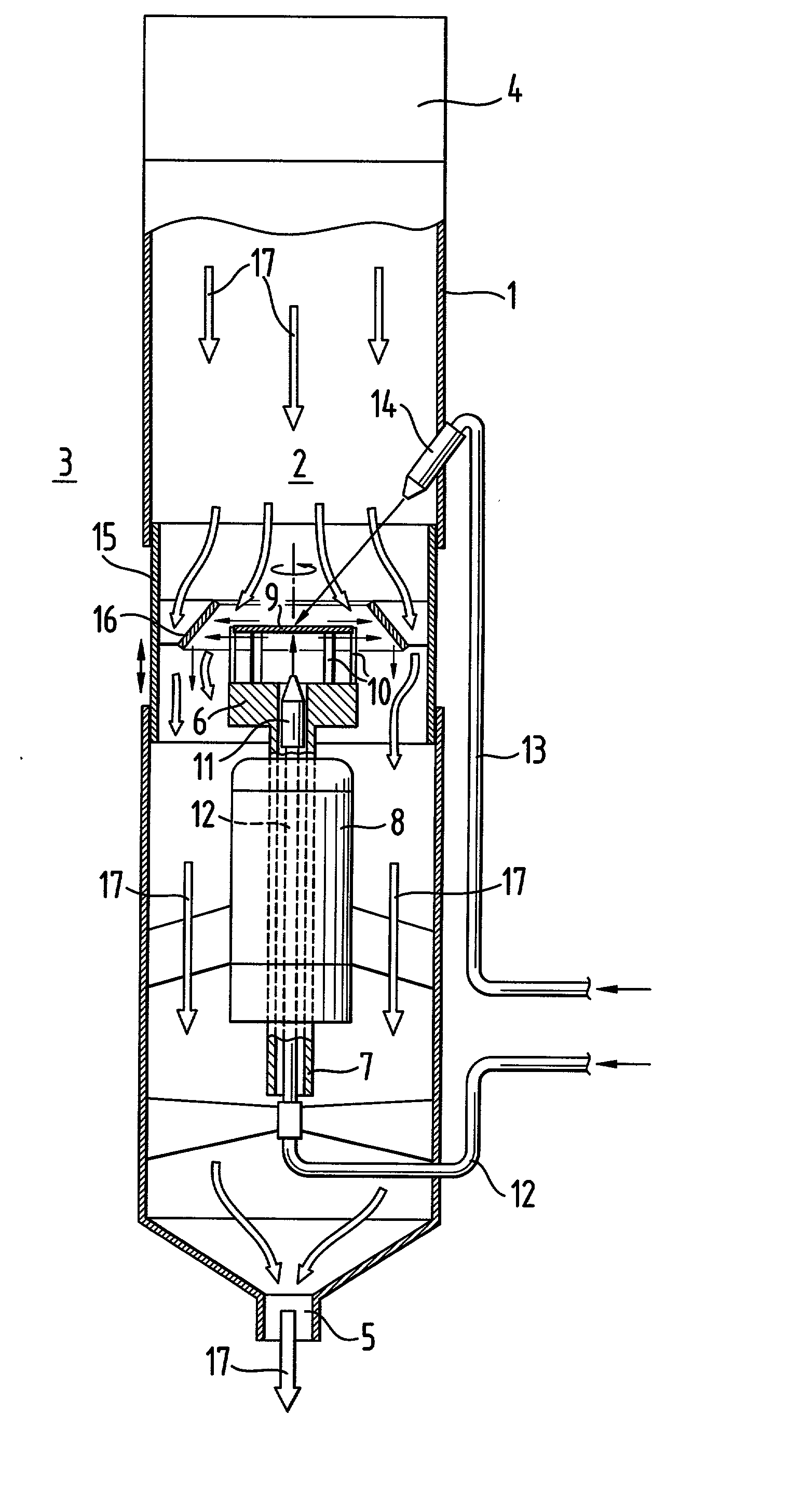
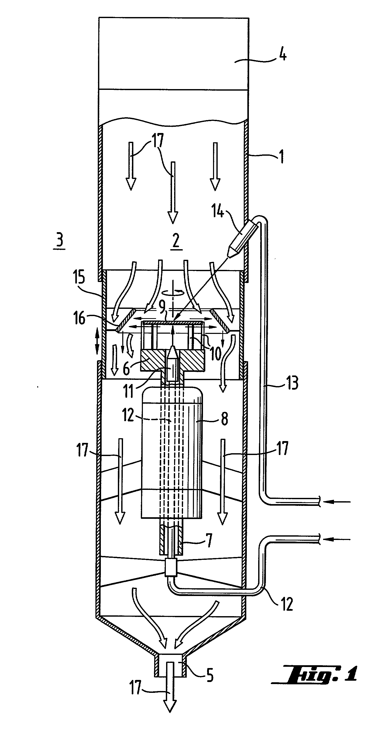
[0028] a) Placing a damp semiconductor wafer, to which chemicals may have been applied, on a centrifuge. Fixing the semiconductor wafer by clamping the semiconductor wafer at a number of points on its edge.

[0029] b) Rinsing centrifuging of the semiconductor wafer. A rinsing agent, for example water, is applied to the top side and the underside of the semiconductor wafer via nozzles. The shape of the nozzles is selected in such a manner that the medium strikes the semiconductor wafer at least in the center, and preferably from the center to the edge. The minimum amount of water dispensed is preferably from 0.1 to 4.0 l / min per nozzle. During the rinsing period, the wafer is accelerated to a desired maximum speed once it has passed through one or more ramps. As shown ...


PUM

PropertyMeasurementUnit
Distanceaaaaaaaaaa
Distanceaaaaaaaaaa
Speedaaaaaaaaaa

Abstract

A centrifuge for a semiconductor wafer has a centrifuge plate for holding a semiconductor wafer, has a drive for setting the centrifuge plate in rotation, and has a device for supplying a medium to a front side and a rear side of the semiconductor wafer. The centrifuge has a housing which separates a centrifuging area and the semiconductor wafer from the environment, and a device for generating a laminar gas flow in the housing. A method for centrifuging a semiconductor wafer has the semiconductor wafer being centrifuged in a laminar gas flow.

Description

[0001] 1. Field of the Invention[0002] The present invention relates to a centrifuge for a semiconductor wafer and a centrifuging method carried out therewith.[0003] 2. The Prior Art[0004] Centrifuges for semiconductor wafers are known. For example, EP-434,307 A2 describes a centrifuge which is used for drying a semiconductor wafer.[0005] When using such a centrifuge, there is a risk of the semiconductor wafer being contaminated during centrifuging, for example by particles which emanate from the centrifuge. Rebounding of drops which have been centrifuged off onto dry points on the semiconductor wafer may also lead to recontamination.[0006] It is an object of the present invention to provide an improved centrifuge in which this risk of recontamination is substantially eliminated.[0007] A further object of the present invention is a method for centrifuging a semiconductor wafer, wherein the semiconductor wafer is centrifuged in a laminar gas flow.[0008] The above objects are achieved...

Claims


Application Information

Patent Timeline
IPC IPC(8): H01L21/304C30B33/00F26B5/08H01L21/00
CPCC30B33/00Y10S134/902H01L21/67034
Inventor HOHL, GEORG-FRIEDRICHBRUNNER, ROLANDBAUER-MAYER, SUSANNEBRUNNER, GUNTHERLUTHE, HANS-JOACHIMSOLLINGER, FRANZ
Owner SILTRONIC AG
Why Eureka
Try Eureka