Dielectric filter, dielectric duplexer, and communication apparatus incorporating the same
- Summary
- Abstract
- Description
- Claims
- Application Information
AI Technical Summary
Benefits of technology
Problems solved by technology
Method used
Image


Examples
first embodiment
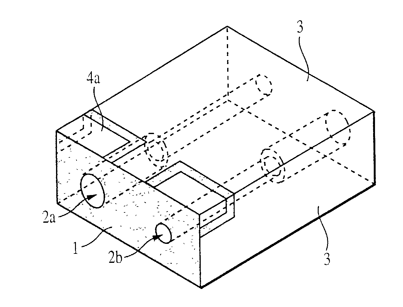
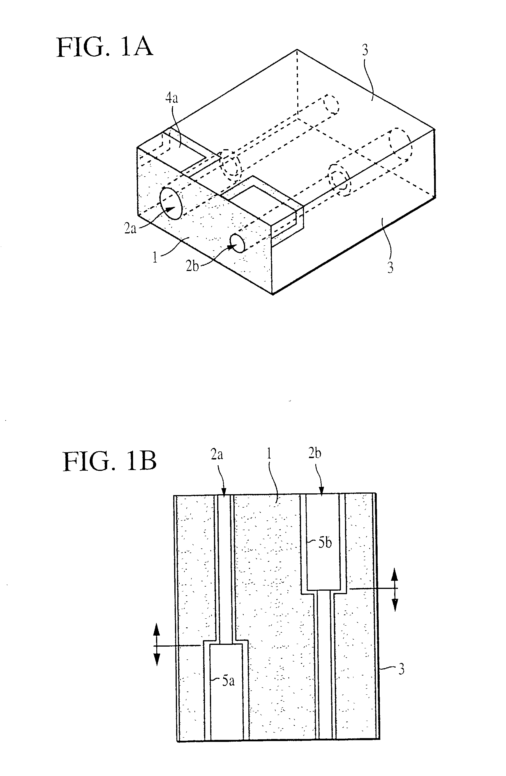
[0029] A description will be given of the structure of a dielectric filter according to the present invention with reference to FIGS. 1A and 1B.
[0030] FIG. 1A shows a perspective view of the dielectric filter, in which the top surface is the surface to be mounted on a circuit board. FIG. 1B shows a sectional view taken along a plane parallel to the mounting surface. In this figure, the reference numeral 1 denotes a substantially rectangular-parallelepiped dielectric block, inside which resonance line holes 2a and 2b are formed. The resonance line holes 2a and 2b are through-holes penetrating two substantially parallel opposing end surfaces of the dielectric block 1. The inner diameter of each of the through-holes 2a and 2b is changed at a specified position in the axial direction of the holes to form a stepped part. Hereinafter, the small inner-diameter part is referred to as a small diameter part and the large inner-diameter part is referred to as a large diameter part.
[0031] By di...
second embodiment
[0037] Next, the structure of a dielectric filter according to the present invention will be illustrated with reference to FIGS. 2A to 2C.
[0038] FIG. 2A shows a back view of the dielectric filter, FIG. 2B shows a sectional view taken along a plane parallel to the mounting surface of the dielectric filter, and FIG. 2C shows a front view of the dielectric filter. Unlike the example shown in FIGS. 1A and 1B, an outer conductor 3 is also formed on the dielectric block at the two opening ends of resonance line holes 2a and 2b. Inside the resonance line holes near the opening ends, electrodeless portions g are formed, whereby a stray capacitance is generated at each of the electrodeless portions g. This arrangement provides a structure in which a capacitance is connected between both ends of each of the resonance lines 5a and 5b and ground. As a result, the two resonators have electromagnetic-field coupling.
third embodiment
[0039] FIGS. 3A, 3B, and 3C are views showing the structure of a dielectric filter according to the present invention. FIG. 3A is a back view of the dielectric filter, FIG. 3B is a sectional view taken along a plane parallel to a surface to be mounted, and FIG. 3C is a front view of the dielectric filter. Unlike the example shown in FIGS. 1A and 1B, a resonance line hole 2b has stepped parts in two positions in the axial direction thereof. In this way, by widening the inner diameters near both open-circuited ends of the resonance line hole 2b, the resonance frequency of a resonance line 5b is lowered, and the capacitive coupling between resonators can be enhanced.
PUM
 Abstract
Description
Claims
Application Information
 - R&D Engineer
- R&D Manager
- IP Professional
- Industry Leading Data Capabilities
- Powerful AI technology
- Patent DNA Extraction
Browse by: Latest US Patents, China's latest patents, Technical Efficacy Thesaurus, Application Domain, Technology Topic.
© 2024 PatSnap. All rights reserved.Legal|Privacy policy|Modern Slavery Act Transparency Statement|Sitemap