

Light receiving element, light detector with built-in circuitry and optical pickup
a light receiving element and light detector technology, applied in the direction of optical radiation measurement, radiation controlled devices, instruments, etc., can solve the problems of reducing the response speed of the photodiode and the probability of the photodiode failing to read an address signal immediately
- Summary
- Abstract
- Description
- Claims
- Application Information
AI Technical Summary
Problems solved by technology
Method used
Image

Examples
example 2
[0147] FIG. 4A is a cross-sectional view showing a structure of a light receiving element (photodiode) according to Example 2 of the present invention. FIG. 4B is a graph showing the impurity concentration on a cross section of the photodiode, taken along line Y-Y' in FIG. 4A. Note that in FIG. 4A, an anode electrode, a cathode electrode, signal lines and a surface protection film are not shown.
[0148] The photodiode shown in FIG. 4A comprises a semiconductor structure comprising a low resistivity P-type semiconductor substrate 7 (second conductivity type semiconductor layer), and an N++-type buried diffusion layer 6 (first conductivity type semiconductor layer) thereon, which has a higher impurity concentration than that of the low resistivity P-type semiconductor substrate 7. On the N++-type buried diffusion layer 6, a P+-type buried diffusion layer 2 having a lower impurity concentration than that of the N++-type buried diffusion layer 6, a high resistivity P-type epitaxial layer ...
example 3
[0166] FIG. 5A is a cross-sectional view showing a structure of a light receiving element (photodiode) according to Example 3 of the present invention. FIG. 5B is a graph showing the impurity concentration on a cross section of the photodiode, taken along line Z-Z' in FIG. 5A. Note that in FIG. 5A, an anode electrode, a cathode electrode, signal lines and a surface protection film are not shown.
[0167] The photodiode shown in FIG. 5A comprises a semiconductor structure comprising a low resistivity N-type semiconductor substrate 5 (first conductivity type semiconductor layer), and an N++-type buried diffusion layer 6 (first conductivity type semiconductor layer) thereon, which has a higher impurity concentration than that of the low resistivity N-type semiconductor substrate 5. On the N++-type buried diffusion layer 6, a P+-type buried diffusion layer 2 having a lower impurity concentration than that of the N++-type buried diffusion layer 6, a high resistivity P-type epitaxial layer 3...
example 4
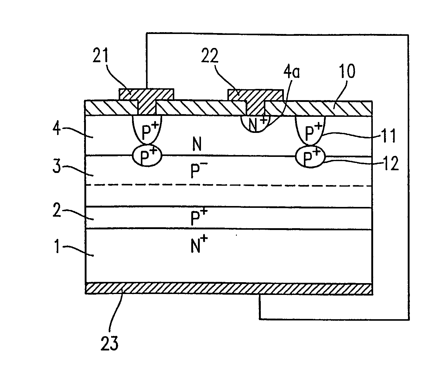
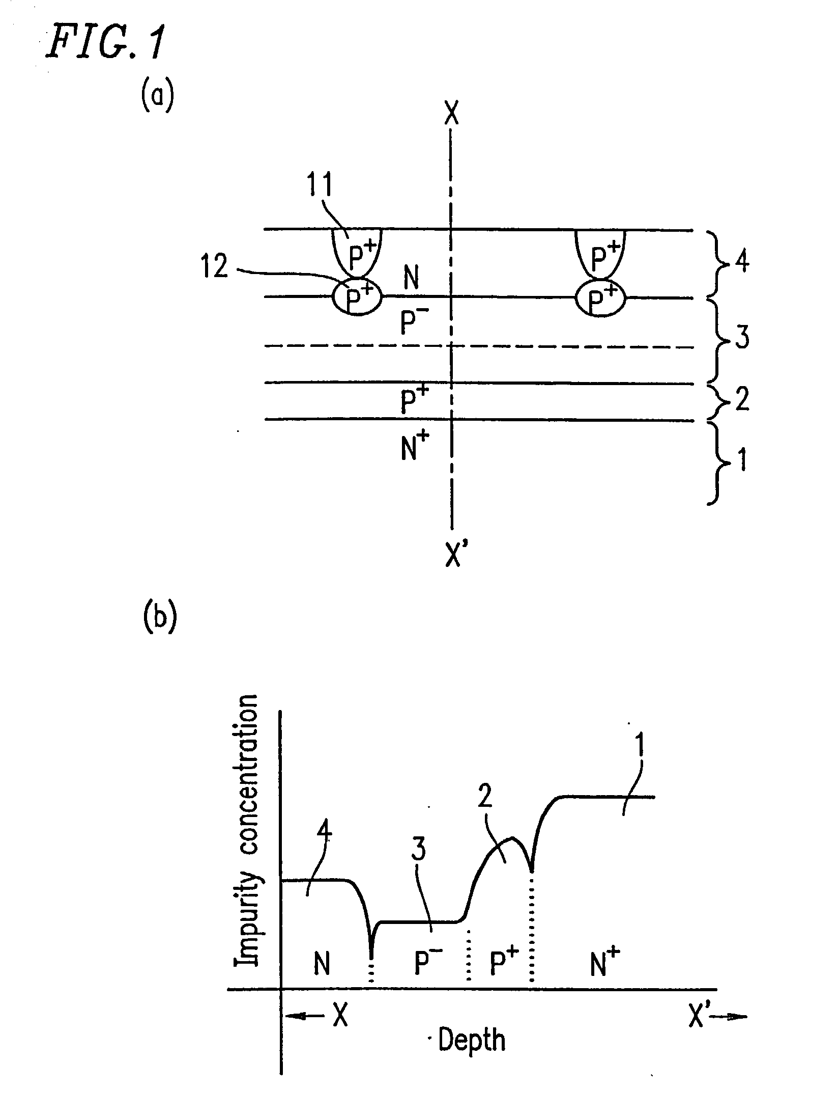
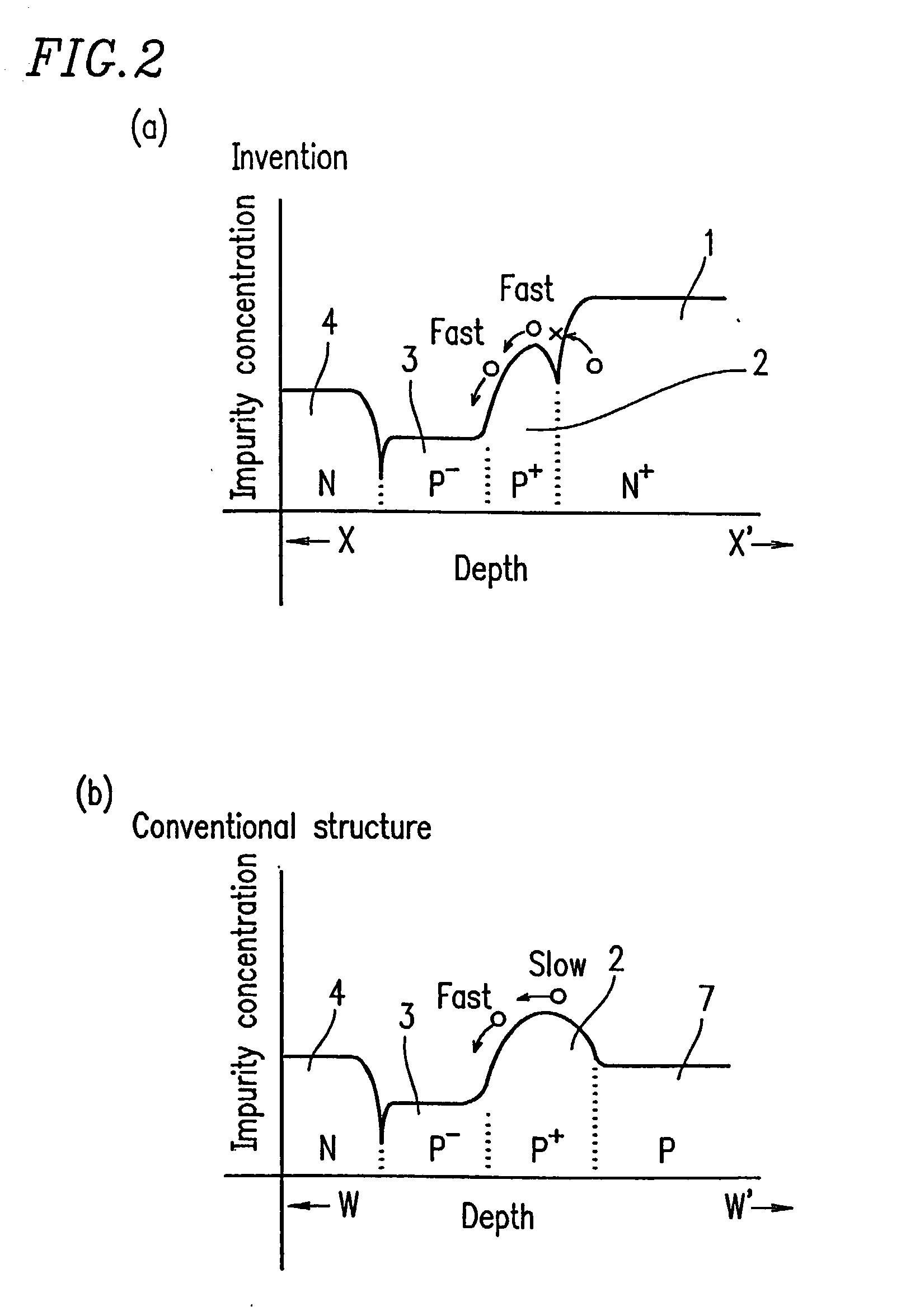
[0185] FIG. 7 is a cross-sectional view showing a light receiving element (photodiode) according to Example 4 of the present invention.
[0186] The photodiode of FIG. 7 comprises an N+-type semiconductor substrate 1 having an impurity concentration, and a P+-type buried diffusion layer 2 having a lower impurity concentration than that of the substrate 1, a high resistivity P-type epitaxial layer 3 having a lower impurity concentration than that of the P+-type buried diffusion layer 2, and an N-type epitaxial layer 4, which are laminated in this order on the substrate 1. Thus, the photodiode has a multilayer structure. A plurality of P+-type separation buried diffusion layers 12 are provided in predetermined regions at an interface between the high resistivity P-type epitaxial layer 3 and the N-type epitaxial layer 4. A P+-type separation buried diffusion layer 11 is provided on each P+-type separation buried diffusion layer 12 within the N-type epitaxial layer 4. A surface of the P+-t...
PUM
 Abstract
Description
Claims
Application Information