Soft convex adhesive wafer
- Summary
- Abstract
- Description
- Claims
- Application Information
AI Technical Summary
Benefits of technology
Problems solved by technology
Method used
Image
Examples
Embodiment Construction
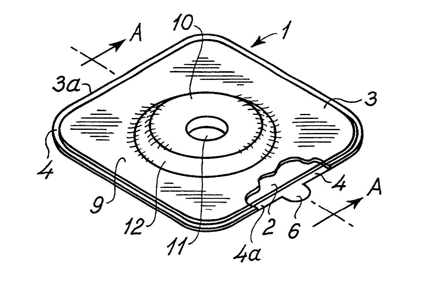
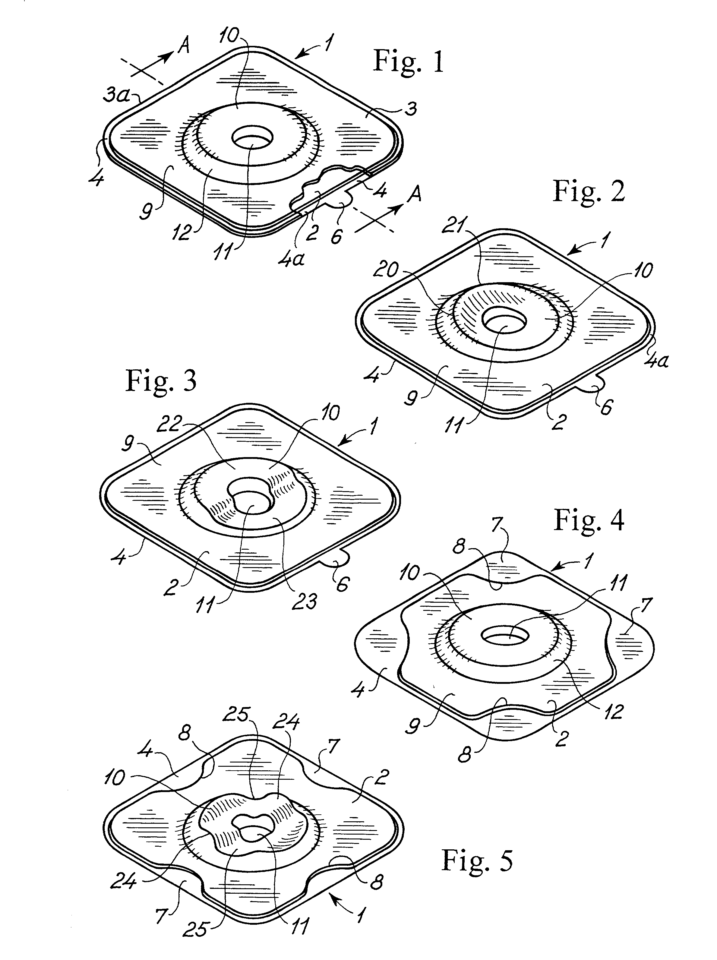
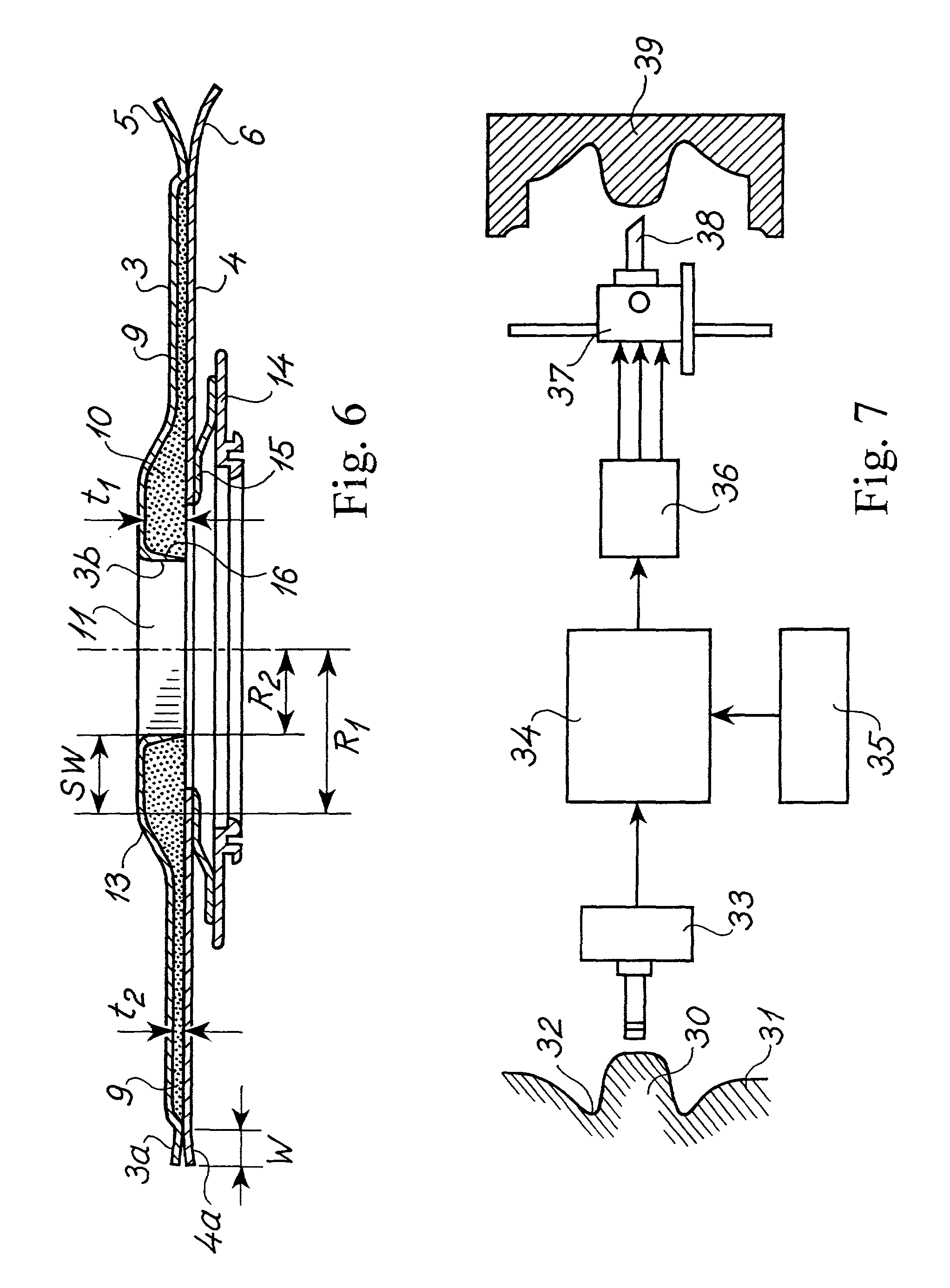
[0084] In the currently preferred set of wafers of the type shown in FIGS. 1 and 6, the thickness t2 is 0.85 mm. The thickness t2 may be larger or smaller if necessary.
[0085] The currently preferred set of wafers of the type shown in FIGS. 1 and 6 are as specified below:
1 R1 No. Wafer Size (mm .times. mm) (mm) t1 (mm) R2 (mm) SW (mm) 1 100 .times. 100 22.0 3.85 12.5 9.5 2 100 .times. 100 18.5 5.85 9.0 9.5 3 100 .times. 100 18.5 5.85 11.5 8.0 4 100 .times. 100 22.0 5.85 12.5 9.5 5 100 .times. 100 22.0 5.85 14.0 8.0 6 115 .times. 115 25.0 3.85 16.0 9.0 7 115 .times. 115 25.0 3.85 17.5 7.5 8 115 .times. 115 25.0 5.85 16.0 9.0 9 115 .times. 115 25.0 5.85 17.5 7.5 10 115 .times. 115 27.5 5.85 19.0 8.5
[0086] The wafer size indicated above is in reality the size of the adhesive layer 2, while the sizes of the wafers 1 including the borders 3a and 4a with a width W of mm are 6 mm larger on each side, i.e. 106 m.times.106 mm and 121 mm.times.121 mm, respectively.
[0087] The set may also compr...
PUM
| Property | Measurement | Unit |
|---|---|---|
| Length | aaaaa | aaaaa |
| Length | aaaaa | aaaaa |
| Length | aaaaa | aaaaa |
Abstract
Description
Claims
Application Information


