High speed switching mosfets using multi-parallel die packages with/without special leadframes

Inactive Publication Date: 2003-10-02
ALPHA & OMEGA SEMICON LTD
View PDF4 Cites 44 Cited by
  • Summary
  • Abstract
  • Description
  • Claims
  • Application Information

AI Technical Summary

Benefits of technology

0010] Specifically, it is an object of the present invention to provide an improved MOSFET device layout and packaging configuration wherein multiple parallel MOSFET chips are connected using an extra gate pad to allow the gate pad of one MOSFET to be wired to that of the other. A low resistance wide metal bus connects the two gate pads on the MOSFET to minimize gate resistance. Significant improvement of package resistance and inductance is achieved.
0011] Briefly in a preferred embodiment this invention discloses a method for configuring a power MOSFET package by packaging several paralleled and separated MOSFET chips in the assembly. The method further include

Problems solved by technology

One single large pad capable of receiving a wire from the gate lead, and one from

Method used


Image

  • High speed switching mosfets using multi-parallel die packages with/without special leadframes
  • High speed switching mosfets using multi-parallel die packages with/without special leadframes
  • High speed switching mosfets using multi-parallel die packages with/without special leadframes

Examples


Example

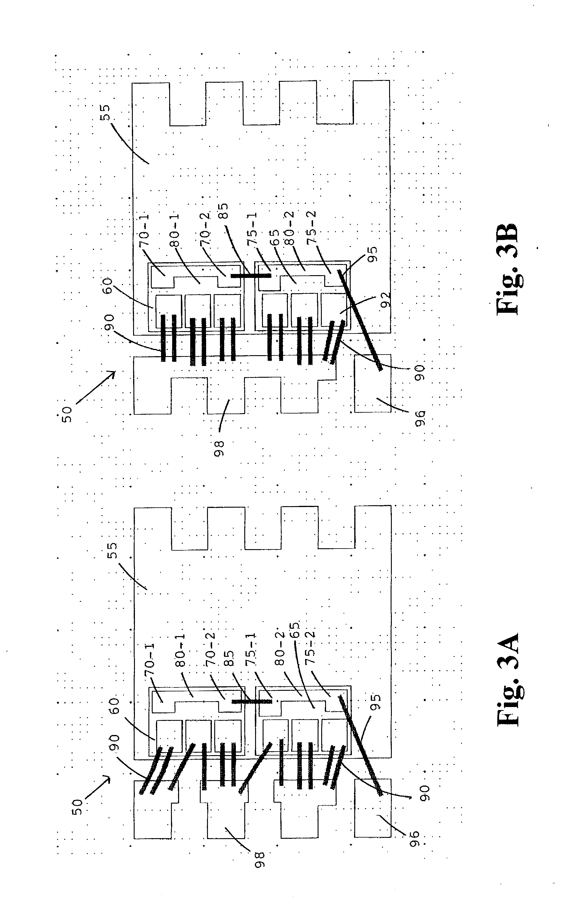
[0019] Referring to FIGS. 3A to 3B for two preferred embodiments of this invention showing the implementation of a multiple-die configuration in the standard SOIC8 MOSFET packages. In FIGS. 3A and 3B, two smaller MOSFET chips 60 and 65 are supported on a package substrate 55. A low resistance gate bus, e.g., gate buses 80-1 and 80-2, is formed for connecting two gate contact pads 70-1 and 70-2 and 75-1 and 75-2 disposed on the top surface for each of these separate MOSFET chips 60 and 65 respectively. An inter-chip gate wire 85 is used to interconnect the gate contacts 70-2 and 75-1 disposed on the separate chips 60 and 65. A common gate wire 95 then connects the gate contact 75-2 to a gate terminal 96 of the MOSFET package 50. A plurality of source wires 90 are connected between the source contacts on the separate chips 60 and 65 and source terminals 98 with and without source leads fused respectively. Unlike the prior art chip arrangement shown in FIGS. 2A and 2B, because of the g...


PUM


Abstract

This invention discloses a method for configuring a power MOSFET package by packaging several paralleled and separated MOSFET chips in the assembly. The method further includes a step of connecting the gate pad on each of these MOSFET chips with a low-resistance gate bus. The package resistance and inductance are significantly reduced and switching speed and heat dissipation are substantially improved.

Description

[0001] This application claims priority to pending U.S. provisional patent application entitled HIGH SPEED SWITCHING MOSFETS USING MULTI-PARALLEL-DIE PACKAGES WITH / WITHOUT SPECIAL LEADFRAMES filed Mar. 31, 2002 by the same inventors of this Application and accorded Serial No. 60 / 369,170, the benefit of its filing date being hereby claimed under Title 35 of the United States Code.[0002] 1. Field of the Invention[0003] The invention disclosed herein relates generally to the device layout and packaging configuration of power MOSFETs. More particularly, this invention relates to a novel and improved device layout and packaging configuration for fabricating and connecting power MOSFETs within electronic packages to achieve high speed switching, reduced power consumption and improved heat dissipation.[0004] 2. Description of the Prior Art[0005] Conventional device layout and packaging configurations for fabricating and connecting a power metal-oxide semiconductor field effect transistor (...

Claims


Application Information

Patent Timeline
IPC IPC(8): H01L23/495H01L25/07
CPCH01L23/49575H01L2924/1306H01L24/49H01L25/072H01L2224/05553H01L2224/05599H01L2224/0603H01L2224/45015H01L2224/45144H01L2224/48091H01L2224/48137H01L2224/48247H01L2224/49111H01L2224/49113H01L2224/49171H01L2224/49175H01L2224/85399H01L2924/01013H01L2924/01014H01L2924/01074H01L2924/01079H01L2924/01082H01L2924/13091H01L2924/14H01L2924/20755H01L2924/30107H01L24/06H01L2924/01033H01L2924/00014H01L2224/45099H01L2924/00H01L2924/00012H01L2224/48111H01L24/48H01L2224/023H01L2924/0001
Inventor BHALLA, ANUPLUI, SIK K.LUO, LEESHAWNHO, YUEH-SE
Owner ALPHA & OMEGA SEMICON LTD
Why Eureka
Try Eureka