Power semiconductor module and power semiconductor device

a technology of power semiconductor and semiconductor device, which is applied in the direction of dc-ac conversion without reversal, frequency selective two-port network, and semiconductor element deformation or breakdown, etc., to achieve the effect of suppressing gate oscillation, reducing gate oscillation, and reducing gate resistance or dispensing

Active Publication Date: 2019-08-01
MITSUBISHI ELECTRIC CORP
View PDF0 Cites 3 Cited by
  • Summary
  • Abstract
  • Description
  • Claims
  • Application Information

AI Technical Summary

Benefits of technology

[0020]According to the power semiconductor module of the present invention, the first external terminal and the second external terminal are electrically connected to the wiring in such a manner that a section electrically connecting the first external terminal and the second external terminal on the wiring which is connected by the respective terminals of the plurality of semiconductor elements operating in parallel includes at least a part of a current-carrying region on the wiring when the first plurality of semiconductor elements are operating in parallel. Thus, a filter may be formed by connecting a filter forming element between the first external terminal and the second external terminal outside the housing so as to reduce the gate oscillation.
[0021]Therefore, according to the power semiconductor module, a filter may be provided and adjusted outside the module so as to suppress the gate oscillation. Further, according to the power semiconductor module, if the filter is provided as described above, the gate resistance may be minimized or dispensed with, which makes it possible to prevent the switching speed from being lowered by the gate resistance. Further effects may be obtained in combination with the gate resistance.
[0022]According to the power semiconductor device of the present invention, the first external terminal and the second external terminal of each of the power semiconductor modules are electrically connected to the wiring in such a manner that a section electrically connecting the first external terminal and the second external terminal on the wiring which is connected by the respective terminals of the plurality of semiconductor elements operating in parallel includes at least a part of a current-carrying region on the wiring when the plurality of semiconductor elements are operating in parallel, and a filter forming element outside the housing is electrically connected between the first external terminal of the first power semiconductor module and the first external terminal of the second power semiconductor module. Thereby, it is possible to form a filter so as to suppress oscillation occurring between the modules and reduce gate oscillation inside each module.
[0023]Therefore, according to the power semiconductor device, a filter may be provided and adjusted outside the module so as to suppress the gate oscillation between the modules and reduce the gate oscillation inside each module. Further, according to the power semiconductor device, if the filter is provided as described above, the gate resistance may be minimized or dispensed with, which makes it possible to prevent the switching speed from being lowered by the gate resistance.

Problems solved by technology

As the number of semiconductor elements operating in parallel increases, the footprint of each element increases and the wiring becomes complicated, which increases the parasitic inductance between the plurality of semiconductor elements operating in parallel.
The gate oscillation may cause the semiconductor elements to degrade or breakdown, and may also cause noises to be radiated to the outside of the module or cause conductive noises in the external circuit, for example.

Method used


Image

  • Power semiconductor module and power semiconductor device
  • Power semiconductor module and power semiconductor device
  • Power semiconductor module and power semiconductor device

Examples


first embodiment

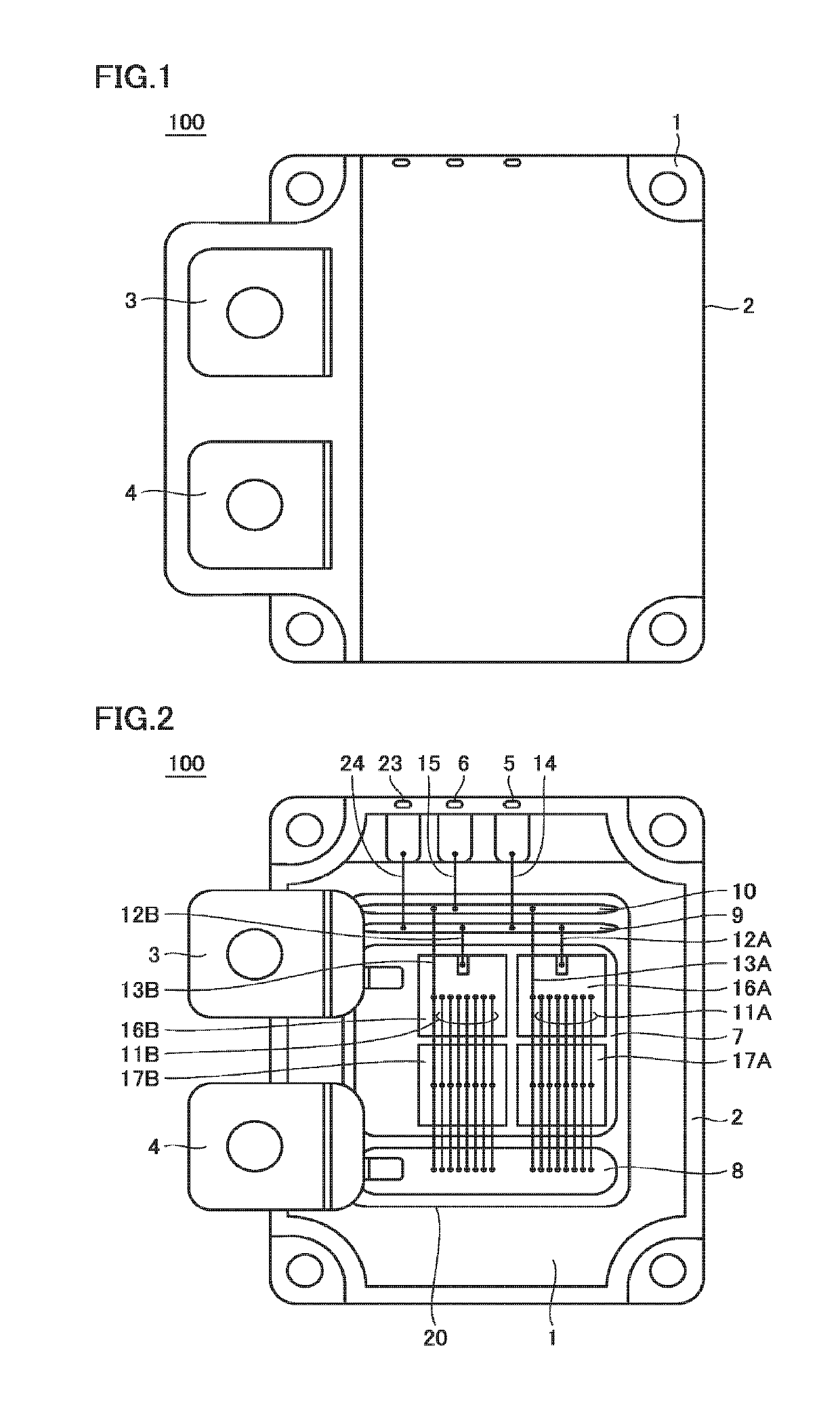
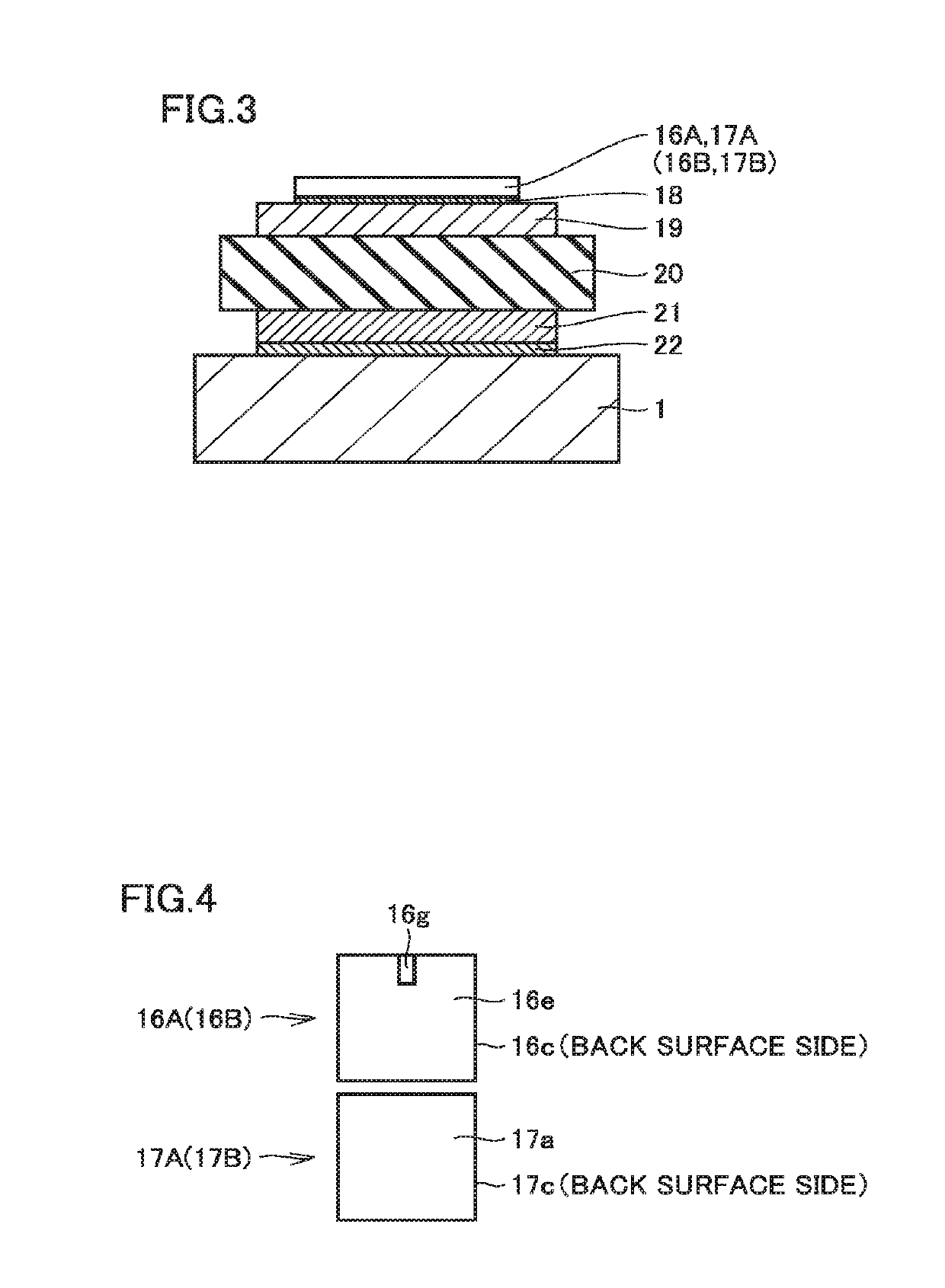
[0050]The configuration of a power semiconductor module according to a first embodiment of the present invention will be described with reference to FIGS. 1 to 4. FIG. 1 is a top view illustrating a power semiconductor module according to the first embodiment, and FIG. 2 is a plan view schematically illustrating the inner configuration of the power semiconductor module illustrated in FIG. 1. FIG. 3 is a cross-sectional view schematically illustrating a part of a cross section of the power semiconductor module illustrated in FIG. 1, and FIG. 4 is a plan view schematically illustrating the configuration of the semiconductor element illustrated in FIG. 1.

[0051]With reference to FIGS. 1 to 4, the power semiconductor module 100 may be appropriately used in a power conversion device such as an inverter or a converter. The power semiconductor module 100 includes a base plate 1, a housing 2, a positive electrode 3, and a negative electrode 4. The base plate 1 is a heat dissipation plate whi...

second embodiment

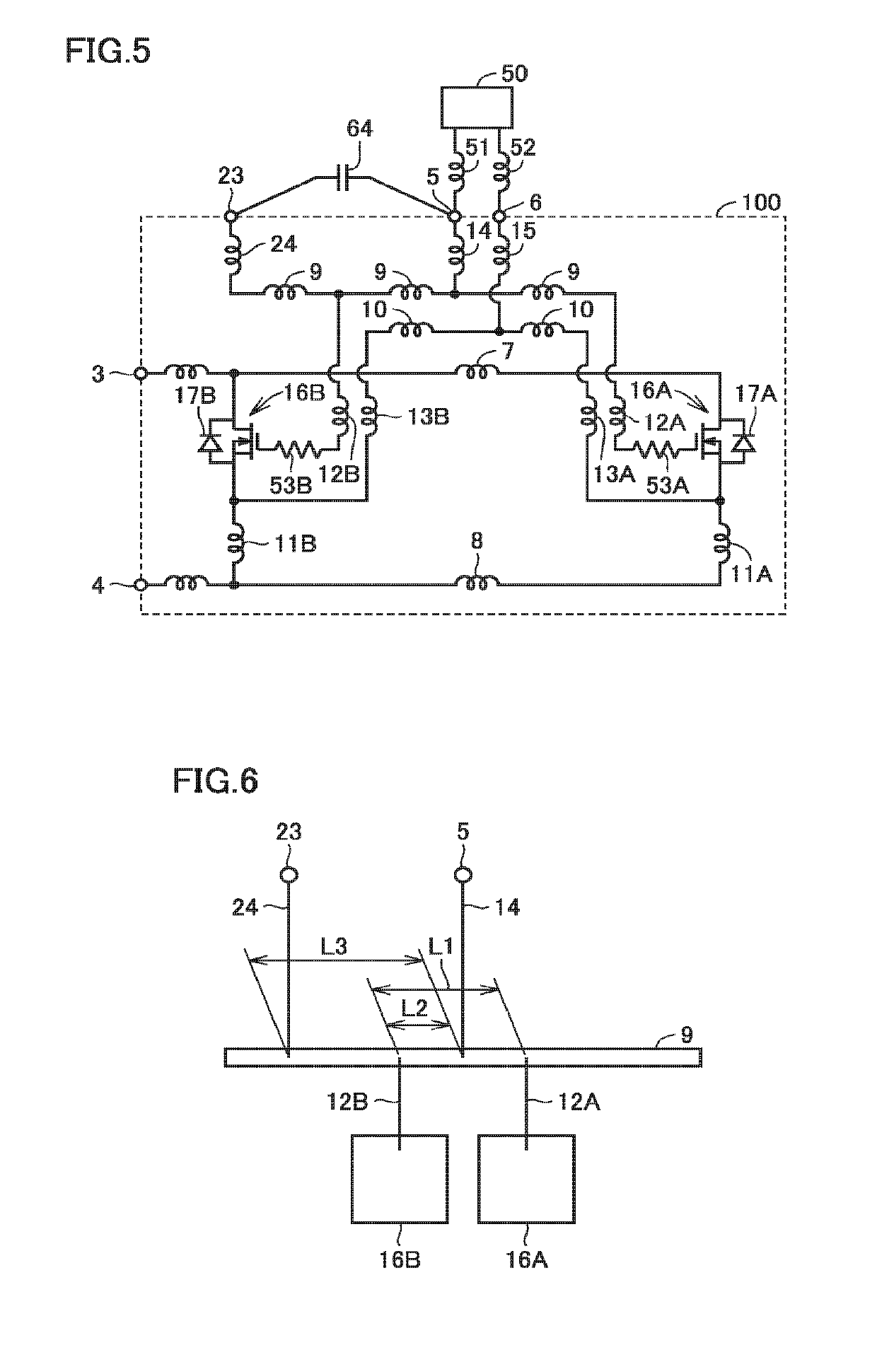
[0095]In the first embodiment mentioned above, it is described that a filter is formed relative to the gate control wiring pattern 9 so as to suppress the gate oscillation. When the semiconductor switching elements 16A and 16B operate in parallel, oscillation may occur between the semiconductor switching elements 16A and 16B due to the parasitic capacitance of the semiconductor switching elements 16A and 16B and the parasitic inductance of the wiring connecting the semiconductor switching elements 16A and 16B. Thus, the collector wiring pattern 7 may become an oscillation path, and the oscillation in the path may result in gate oscillation. Therefore, in the second embodiment, a filter is formed relative to the collector wiring pattern 7 so as to suppress the oscillation.

[0096]In the present embodiment, in order to measure an internal voltage of the power semiconductor module, a collector sensing terminal is provided so as to obtain a potential at a location closer to the semiconduc...

third embodiment

[0106]As described above, when the semiconductor switching elements 16A and 16B operate in parallel, oscillation may occur between the semiconductor switching elements 16A and 16B. Thus, the emitter wiring pattern 8 may become an oscillation path, and the oscillation in the path may result in the gate oscillation. Therefore, in the third embodiment, a filter is formed relative to the emitter wiring pattern 8 so as to suppress the oscillation.

[0107]In the present embodiment, in order to detect a current flowing through the power semiconductor module, an emitter sensing terminal is provided to obtain a potential at a location closer to the semiconductor switching elements 16A, 16B than the negative electrode 4. The emitter sensing terminal is connected to the emitter wiring pattern 8 by wires. When a current flows through the parasitic inductance between the emitter sensing terminal and the negative electrode 4, the voltage drops in accordance with the temporal change of the current a...


PUM


Abstract

Gates of semiconductor switching elements are connected to a gate control wiring pattern. The gate control wiring pattern is further connected to a gate control terminal and a filter terminal which are connected by an element for forming a filter outside a housing. The filter terminal and the gate control terminal are connected to the gate control wiring pattern in such a manner that a section electrically connecting the filter terminal and the gate control terminal overlaps with at least a part of a section electrically connecting the gates of the semiconductor switching elements on the gate control wiring pattern.

Description

TECHNICAL FIELD[0001]The present invention relates to a power semiconductor module and a power semiconductor device, and particularly to a power semiconductor module including a plurality of semiconductor elements operating in parallel and a power semiconductor device including a plurality of power semiconductor modules operating in parallel.BACKGROUND ART[0002]Generally, in an insulated type power semiconductor module used in a power conversion device such as an inverter or a converter, a wiring pattern is formed on an insulating layer provided on a metal plate which serves as a heat radiation plate, and power semiconductor elements such as transistors and diodes are provided on the wiring pattern. Then the power semiconductor elements are connected to an external terminal or the like by wire bonding and sealed with resin, for example.[0003]In order to obtain a power semiconductor module which performs switching operation at a large current, the module is provided with a plurality ...

Claims


Application Information

Patent Timeline
Patent Type & Authority Applications(United States)
IPC IPC(8): H01L25/16H01L25/18H03H7/01H03H7/06H03H11/04H02M7/00
CPCH01L25/16H01L25/18H03H7/0138H03H7/06H03H11/04H02M7/003H01L24/32H01L2224/32225H01L24/48H01L24/49H01L2224/48137H01L2224/48227H01L2224/49175H01L24/73H01L2224/73265H01L2924/1203H01L2924/13055H01L2924/13091H01L2924/10272H01L2924/10254H01L2924/1033H01L23/3675H02M7/48H01L25/07H01L2224/0603H01L2224/48139H01L2224/49111H01L2924/19107H01L25/072H01L2924/00H01L2924/00014H01L2224/48091H02M7/5387H01L2924/00012
Inventor NAKASHIMA, JUNICHITAMADA, YOSHIKONAKAYAMA, YASUSHI
Owner MITSUBISHI ELECTRIC CORP
Why Eureka
Try Eureka