Semiconductor device

a technology of semiconductor devices and signal terminals, applied in semiconductor devices, semiconductor/solid-state device details, electrical apparatus, etc., can solve the problems of abnormal gate oscillation, complex connection structure between signal terminals and external devices, and current variation, so as to suppress abnormal gate oscillation, simplify the connection structure between signal terminals and external devices, and suppress current variation

Active Publication Date: 2019-03-21
DENSO CORP
View PDF0 Cites 5 Cited by
  • Summary
  • Abstract
  • Description
  • Claims
  • Application Information

AI Technical Summary

Benefits of technology

[0019]In accordance with the aspect, in the plurality of semiconductor chips connected in parallel, the pads are formed on the same side of the main electrode, and the corresponding signal terminals extend in the same direction. This allows a connection structure between the signal terminals and the outside to be simplified.
[0020]In addition, each of the inductances of the parallel-connecting parts is smaller than the inductance of the series-connecting part including the joint part. For example, when it is assumed that the inductance of the series-connecting part has a predetermined value, the inductance of each of the parallel-connecting parts can be reduced compared to that in a configuration in which the inductance of the parallel-connecting part is set to be equal to or larger than the inductance of the series-connecting part. This can suppress current variation, while allowing the layout of the pads described above to be used. By satisfying the magnitude relationship between the inductances described above, it is possible to suppress abnormal gate oscillation. Since a gate resistance or the like need not be inserted in a gate, it is possible to suppress abnormal gate oscillation, while suppressing an increase in switching loss. The effect of suppressing abnormal oscillation has been recognized by experiment.

Problems solved by technology

However, when a parallel connection structure is adopted, current variation or abnormal gate oscillation is likely to occur.
However, since the signal terminals in the same arm are extended in the opposite directions, a connection structure between the signal terminals and the outside (external device) is complicated.
However, such countermeasures undesirably increase a switching loss.

Method used


Image

  • Semiconductor device
  • Semiconductor device
  • Semiconductor device

Examples


first embodiment

[0035]First, on the basis of FIG. 1, a description will be given of an example of a power conversion device to which a semiconductor device is applied.

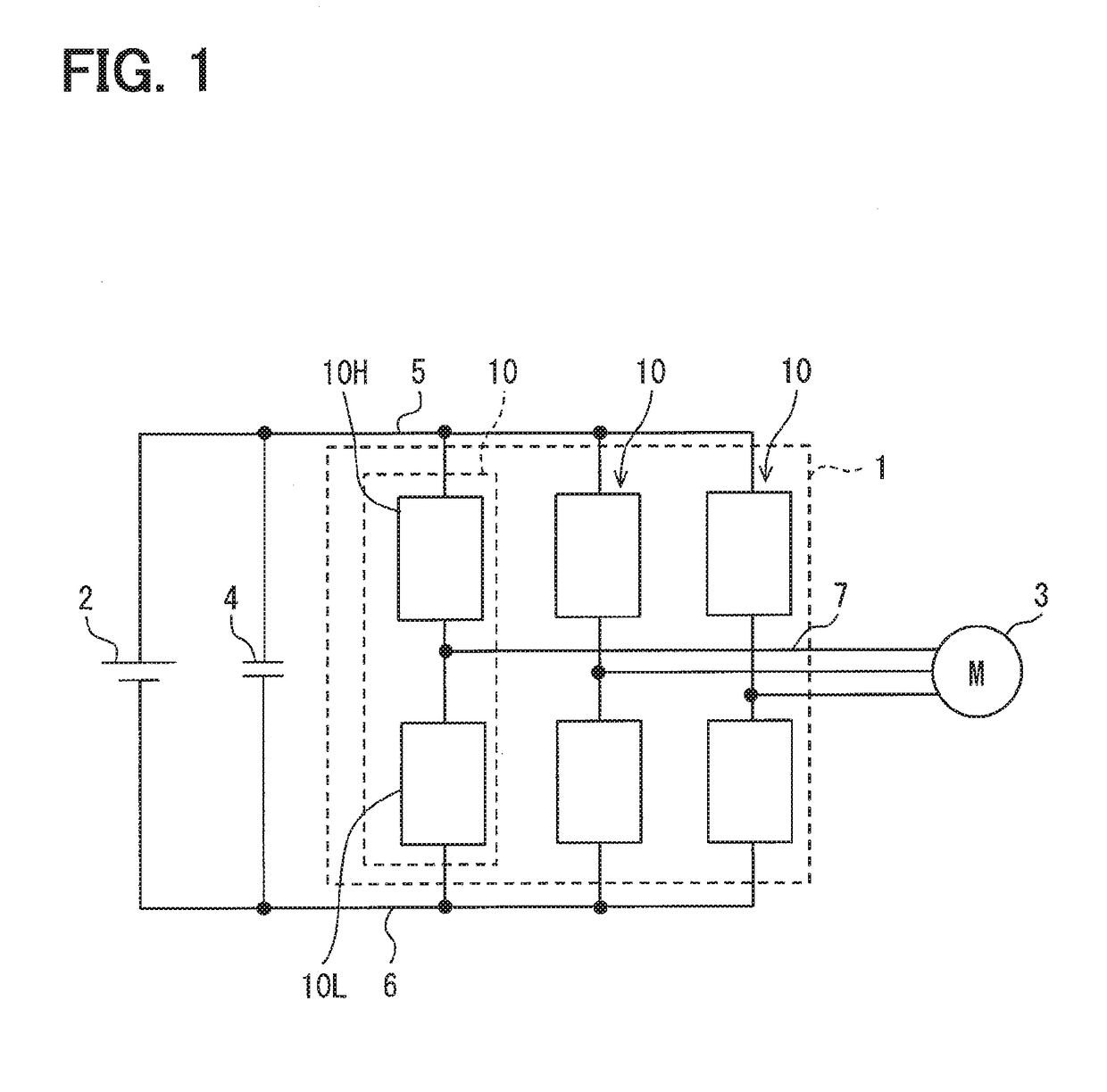
[0036]A power conversion device 1 shown in FIG. 1 is configured so as to convert a DC voltage supplied from a DC power source 2 (battery) to a three-phase AC current and output the three-phase AC current to a three-phase AC motor 3. The power conversion device 1 thus configured is mounted in, e.g., an electric vehicle or a hybrid vehicle. Note that the power conversion device 1 can also convert the power generated by the motor 3 to a DC power and charge the DC power source 2 with the DC power. The reference numeral 4 shown in FIG. 1 denotes a smoothing capacitor.

[0037]The power conversion device 1 has a three-phase inverter. The three-phase inverter has upper and lower arms for three phases, which are provide between a higher-potential power source line 5 connected to the positive (higher-potential) electrode of the DC power source 2 ...

second embodiment

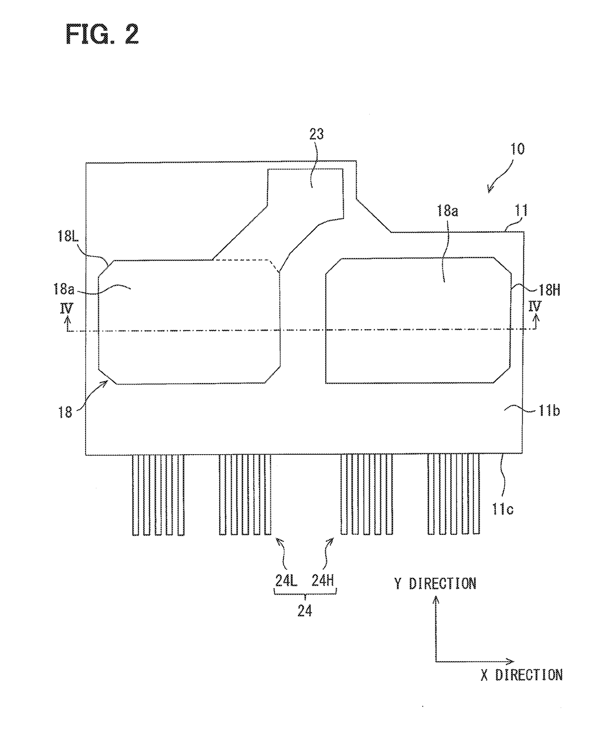
[0100]For the present embodiment, the previous embodiment can be referred to. Accordingly, a description of components which are common to those of the semiconductor device 10 shown in the previous embodiment is omitted.

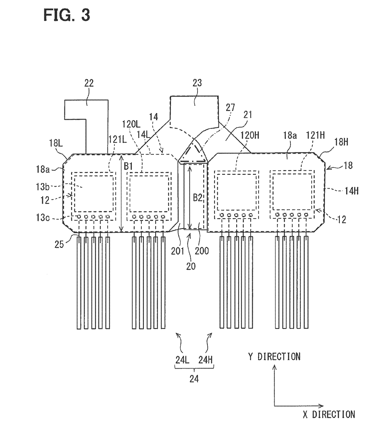
[0101]In the semiconductor device 10 in the present embodiment, the surface of the joint part 20 has an uneven shape. FIG. 8 shows an example of the present embodiment. In FIG. 8, in the portion of the surface of the first joint part 200 connected to a solder which is closer to the end thereof continued to the heat sink 18H, a depressed portion 203 is formed. The depressed portion 203 is formed in the portion of the first joint part 200 which is in contact with the solder 202 to serve as a current path. The depressed portion 203 extends in the Y-direction, though the depiction thereof is omitted. The depressed portion 203 is formed to extend from one end of the first joint part 200 to the other end thereof in the Y-direction. The depressed portion 203 can be formed b...

third embodiment

[0105]For the present embodiment, the previous embodiments can be referred to. Accordingly, a description of components which are common to those of the semiconductor device 10 shown in each of the previous embodiments is omitted.

[0106]In the present embodiment, the joint part 20 has through holes. FIG. 9 shows an example of the present embodiment. In FIG. 9, through holes 204 are formed in the portion of the first joint part 200 which is closer to the end thereof continued to the heat sink 18H. Similarly to the depressed portion 203, the through holes 204 are formed in the portion of the first joint part 200 which is in contact with the solder 202 to serve as the current path. In the first joint part 200, the plurality of through holes 204 are formed, though the depiction thereof is omitted. The plurality of through holes 204 are formed at predetermined intervals in the Y-direction. The through holes 204 can also be formed by, e.g., pressing or etching.

[0107]By thus using the joint...


PUM


Abstract

In a semiconductor device, a plurality of semiconductor chips included in an upper-arm circuit are connected in parallel between a pair of upper-arm plates, while a plurality of semiconductor chips included in a lower-arm circuit are connected in parallel between a pair of lower-arm plates. In each of the arm circuits, the plurality of semiconductor chips are arranged in a direction perpendicular to a direction in which emitter electrodes and pads are arranged, the pads are disposed on the same side of the emitter electrodes, and signal terminals extend in the same direction. A series-connecting part between the upper- and lower-arm circuits includes a joint part 20 continued to respective side surfaces of the corresponding upper- and lower-arm plates. Each of inductances of respective parallel-connecting parts of the upper- and lower-arm plates which connect the semiconductor chips in parallel is smaller than an inductance of the series-connecting part.

Description

CROSS REFERENCE TO RELATED APPLICATION[0001]This application is based on Japanese Patent Application No. 2016-101245 filed on May 20, 2016, the disclosure of which is incorporated herein by reference.TECHNICAL FIELD[0002]The present disclosure relates to a semiconductor device having a double-surface heat dissipation structure.BACKGROUND ART[0003]As disclosed in Patent Literature 1, a semiconductor device having a double-surface heat dissipation structure is known in which an upper-arm chip included in an upper-arm circuit is disposed between a pair of upper-arm plates, a lower-arm chip included in a lower arm is disposed between a pair of lower-arm plates, and the upper-arm circuit and a lower-arm circuit are connected via a joint part. In this semiconductor device, the one upper-arm chip is disposed between the upper-arm plates, while the one lower-arm chip is disposed between the lower-arm plates.PRIOR ART LITERATUREPatent Literature[0004]Patent Literature 1: JP 2016-4941 ASUMMAR...

Claims


Application Information

Patent Timeline
Patent Type & Authority Applications(United States)
IPC IPC(8): H01L23/36H01L25/07H02M7/48H01L23/00
CPCH01L23/36H01L25/07H02M7/48H01L24/42H01L2224/33H01L2224/48247H01L2224/49175H01L2924/181H02M7/003H01L23/4334H01L23/49568H01L23/49537H01L23/49562H01L23/49575H01L2924/13055H01L2224/45124H01L24/45H01L2224/0603H01L2224/05554H01L2224/33181H01L24/48H01L24/49H01L2924/1203H01L2924/13091H01L2224/05553H01L2224/29101H01L2224/40245H01L2224/40139H01L2224/84801H01L2224/83801H01L24/83H01L24/84H01L24/40H01L24/33H01L24/06H01L2924/00014H01L2224/04026H01L2224/04042H01L2224/2612H01L2224/73221H01L2924/00012H01L2924/00H01L2924/014H01L2224/05599H01L25/18
Inventor ISHINO, HIROSHIKAWAHARA, HIDEKIHIRAMITSU, SHINJIARAI, SHUNSUKE
Owner DENSO CORP
Why Eureka
Try Eureka