Memory device

Active Publication Date: 2021-10-21
YANGTZE MEMORY TECH CO LTD
View PDF6 Cites 1 Cited by
  • Summary
  • Abstract
  • Description
  • Claims
  • Application Information

AI Technical Summary

Benefits of technology

The present patent provides a memory device with a vertical transistor that can be connected to a word line structure on another substrate, reducing the area occupied by the vertical transistor and simplifying the connection structure. The vertical transistor includes a semiconductor channel and a gate electrode, and is electrically connected to the word line structure through a conductive line and a connection structure. The memory device also includes a first memory array and a second memory array, with the second memory array being disposed between the first and third substrates in the vertical direction. The technical effects of the present patent include reducing the size of the memory device and simplifying the connection structure between the vertical transistor and the word line structure.

Problems solved by technology

However, as feature sizes of the memory cells approach a lower limit, planar process and fabrication techniques become challenging and costly.
As a result, memory density for planar memory cells approaches an upper limit.
As the dimension of the memory device becomes smaller and the memory cell density becomes higher, the interconnection structure between the memory array and the peripheral devices becomes more complicated and influences the related circuit design and / or the related manufacturing processes.

Method used


Image

  • Memory device
  • Memory device
  • Memory device

Examples


first embodiment

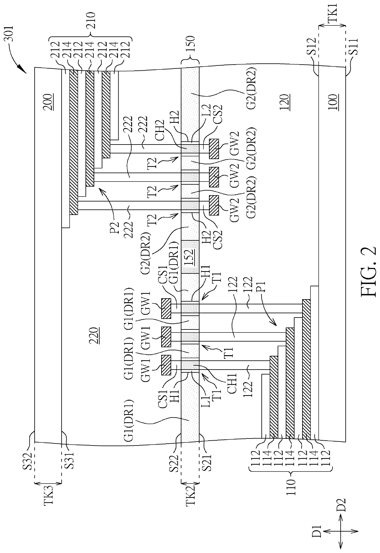
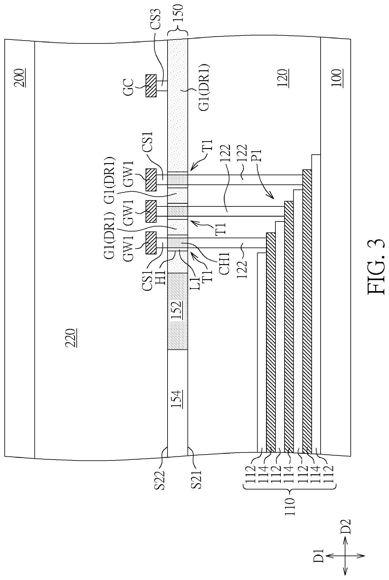
[0047]Please refer to FIG. 2. FIG. 2 is a schematic drawing illustrating a memory device 301 according to the present disclosure. As shown in FIG. 2, the memory device 301 includes a first substrate 100, a first memory array 110, a second substrate 150, and at least one first vertical transistor T1. The first memory array 110 is disposed on the first substrate 100. The first memory array 110 includes at least one first word line structure 114. The first memory array 110 is disposed between the first substrate 100 and the second substrate 150 in a vertical direction (such as a first direction D1 shown in FIG. 2). The first vertical transistor T1 is electrically connected with the first word line structure 114. At least a part of the first vertical transistor T1 is disposed in the second substrate 150. The area occupied by the first vertical transistor T1 on the second substrate 150 may be relatively smaller than the area occupied by the planar transistor described above, and that wil...

second embodiment

[0066]Please refer to FIG. 5. FIG. 5 is a schematic drawing illustrating a memory device 302 according to the present disclosure. As shown in FIG. 5, in the memory device 302, the second memory array 210 may be disposed on the second substrate 150, a part of the second interlay dielectric 220 may be disposed between the second memory array 210 and the third substrate 200 in the first direction D1, and at least a part of each of the second vertical transistors T2 may be disposed in the third substrate 200. In some embodiments, the second semiconductor channel CH2 may penetrate the third substrate 200 in the first direction D1, the second gate electrode G2 may be disposed in the third substrate 200 and surround the second semiconductor channel CH2 in the horizontal direction, and the second gate dielectric layer L2 may be disposed in the third substrate 200 and disposed between the second gate electrode G2 and the second semiconductor channel CH2, but not limited thereto. In some embo...

third embodiment

[0068]Please refer to FIG. 6. FIG. 6 is a schematic drawing illustrating a memory device 303 according to the present disclosure. As shown in FIG. 6, in the memory device 303, the third substrate 200 may be disposed between the first substrate 100 and the second substrate 150 in the first direction D1, and the second memory array 210 may be disposed between the second substrate 150 and the third substrate 200 in the first direction D1. In some embodiments, the second memory array 210 may be disposed on the third substrate 200 and disposed at the second side S32 of the third substrate 200 and the first side S21 of the second substrate 150, and the first conductive lines GW1, the second conductive lines GW2, the first connection structures CS1, the second connection structures CS2, and the protection layer 230 may be disposed on the second substrate 150 and disposed at the second side S22 of the second substrate 150. In some embodiments, the memory device 303 may further include a plu...


PUM


Abstract

A memory device includes a first substrate, a first memory array, a second substrate, and at least one first vertical transistor. The first memory array is disposed on the first substrate. The first memory array includes at least one first word line structure. The first memory array is disposed between the first substrate and the second substrate in a vertical direction. The first vertical transistor is electrically connected with the first word line structure. At least a part of the at least one first vertical transistor is disposed in the second substrate.

Description

CROSS REFERENCE TO RELATED APPLICATIONS[0001]This application is a continuation of International Application No. PCT / CN2020 / 085356 filed on Apr. 17, 2020, which is incorporated herein by reference in its entirety.BACKGROUND OF THE INVENTION1. Field of the Invention[0002]The present disclosure relates to a memory device, and more particularly, to a memory device including a vertical transistor.2. Description of the Prior Art[0003]Planar memory cells are scaled to smaller sizes by improving process technology, circuit design, programming algorithm, and fabrication process. However, as feature sizes of the memory cells approach a lower limit, planar process and fabrication techniques become challenging and costly. As a result, memory density for planar memory cells approaches an upper limit.[0004]A three-dimensional (3D) memory architecture can address the density limitation in planar memory cells. The 3D memory architecture includes a memory array and peripheral devices for controllin...

Claims


Application Information

Patent Timeline
IPC IPC(8): G11C8/08H01L27/24
CPCG11C8/08H01L27/2454H01L29/7827H10B41/35H10B41/20H10B43/35H10B43/20H10B12/50H10B41/40H10B41/50H10B43/50H10B43/40H01L25/0657H10B80/00H10B63/34
Inventor TANG, QIANGHOU, CHUNYUAN
Owner YANGTZE MEMORY TECH CO LTD
Why Eureka
Try Eureka