Semiconductor super junction power device

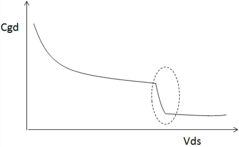
A technology for power devices and semiconductors, applied in semiconductor devices, electrical components, circuits, etc., can solve the problem of insufficient improvement of gate oscillation of superjunction power devices, and achieve reduction of sudden changes, gate-drain capacitance, and gate-drain capacitance sudden changes. smooth effect

Inactive Publication Date: 2017-09-01
SUZHOU ORIENTAL SEMICONDUCTOR CO LTD
View PDF6 Cites 6 Cited by
  • Summary
  • Abstract
  • Description
  • Claims
  • Application Information

AI Technical Summary

Problems solved by technology

However, the improvement of the gate oscillation of super-junction power devices by this scheme is not obvious enough

Method used


Image

  • Semiconductor super junction power device
  • Semiconductor super junction power device
  • Semiconductor super junction power device

Examples


Embodiment Construction

[0024] Combine below Attached picture And embodiment, the specific embodiment of the present invention is described in further detail.

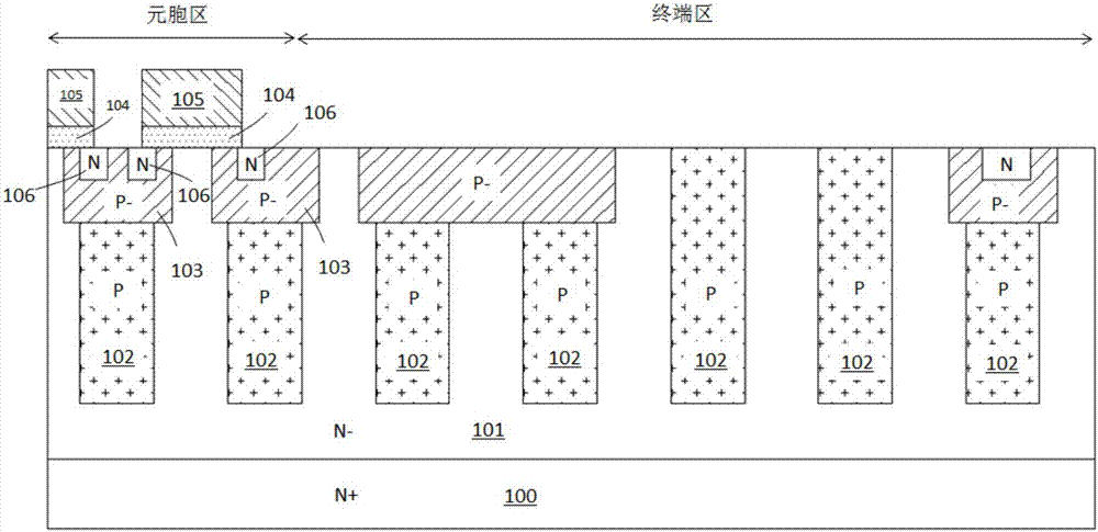
[0025] In order to clearly illustrate the specific implementation of the present invention, the specification In the attached picture Listed indications picture , the thickness of the layer and region described in the present invention is enlarged, and the listed figure size does not represent the actual size; Attached picture are illustrative and should not limit the scope of the invention. The examples listed in the description should not be limited to the description In the attached picture The specific shape of the region shown, but includes the obtained shape such as manufacturing deviations, etc. For example, the curve obtained by etching usually has a curved or rounded feature, which is represented by a rectangle in the embodiment of the present invention.

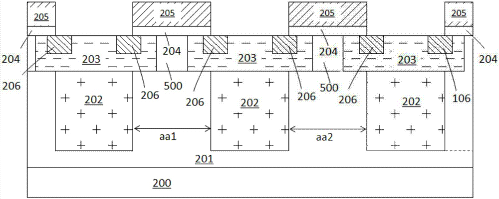
[0026] A semiconductor super junction power device structure proposed...


PUM


Abstract

The invention belongs to the technical field of semiconductor power devices, and particularly relates to a semiconductor super junction power device. The device comprises a terminal region and a cellular region. The cellular region comprises a drain region in a substrate epitaxial layer, a JFET region, and multiple vertical parallel columnar doped regions. The top of each columnar doped region is provided with a body region. Each body region is internally provided with source regions. A gate oxide layer is arranged on the body regions and the JFET region. Gates are arranged on the gate oxide layer. There are two or more kinds of spacing of different width between the adjacent columnar doped regions, and the body regions have two or more kinds of different width. Under the synergistic action of the columnar doped region structures with different spacing and the body region structures of different width, more slow change can be introduced to the super junction power device, gate-drain capacitance mutation becomes smoother, and gate turbulence caused by gate-drain capacitance mutation is reduced.

Description

technical field [0001] The invention belongs to the technical field of semiconductor power devices, in particular to a semiconductor superjunction power device. Background technique [0002] Super-junction power devices are based on charge balance technology, which can reduce on-resistance and parasitic capacitance, so that super-junction power devices have extremely fast switching characteristics, which can reduce switching losses and achieve higher power conversion efficiency. as shown in the picture 1 As shown, the known super junction power device includes a cell region and a terminal region, the cell region is used to obtain low on-resistance, and the terminal region is used to obtain high withstand voltage. The number of columnar doped regions 102 in the terminal region of the device is different according to the specific requirements of the product, which is mainly used for the withstand voltage requirements of different products. The cell region of the device inclu...

Claims


Application Information

Patent Timeline
Patent Type & Authority Applications(China)
IPC IPC(8): H01L29/78H01L29/06H01L29/423
CPCH01L29/0634H01L29/0684H01L29/42356H01L29/7828
Inventor 刘磊王鹏飞袁愿林龚轶
Owner SUZHOU ORIENTAL SEMICONDUCTOR CO LTD
Why Eureka
Try Eureka