Method for manufacturing semiconductor device

a manufacturing method and semiconductor technology, applied in the direction of semiconductor devices, basic electric elements, electrical appliances, etc., can solve the problems of substantial complexity in the formation of the gate stack, inability to meet and the implementation of a dual work function metal gate to satisfy the work function requirements of both pmos and nmos may be substantially difficult, so as to achieve the effect of substantially ensuring the gate conductivity and minimizing the resistance of the ga

Active Publication Date: 2015-08-27
SEMICON MFG INT (SHANGHAI) CORP
View PDF7 Cites 30 Cited by
  • Summary
  • Abstract
  • Description
  • Claims
  • Application Information

AI Technical Summary

Benefits of technology

[0032]According to embodiments of the invention, portions of the high-k layers positioned at sides of gate trenches may be sufficiently removed. Therefore, minimum or substantially no unwanted high-k material residual may exist at contact interfaces of the subsequently formed metal gates. Advantageously, gate resistance may be minimized, and satisfactory gate conductivity may be substantially ensured.

Problems solved by technology

This arrangement may substantially complicate the formation of the gate stack, especially for manufacturing a semiconductor device with feature sizes less than 20 nm.
In the process, implementation of a dual work function metal gate to satisfy work function requirements associated with both the PMOS and NMOS may be substantially difficult.
If the gate stack structure at the NMOS region and the gate stack structure at the PMOS region are manufactured at the same time, the EOT thickness at the NMOS region and the EOT thickness at the PMOS region may not be differently configured and optimized, such that the performance of the semiconductor device may not be optimal.
If the NMOS gate stack and the PMOS gate stack are manufactured separately according to well-known processes, unwanted residual high-k material may remain at contact interfaces of metal gates in the semiconductor device, resulting in undesirable high gate resistance.

Method used


Image

  • Method for manufacturing semiconductor device
  • Method for manufacturing semiconductor device
  • Method for manufacturing semiconductor device

Examples


Embodiment Construction

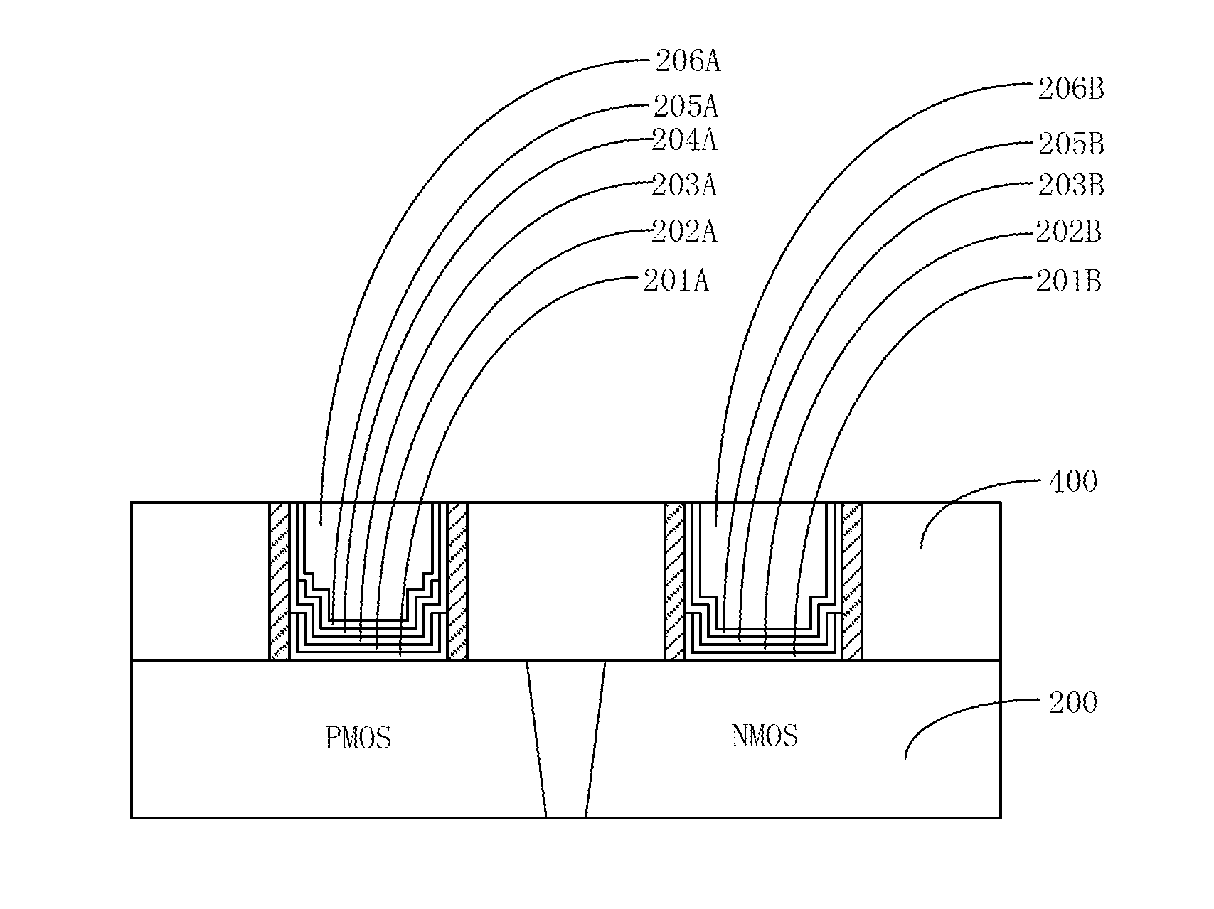
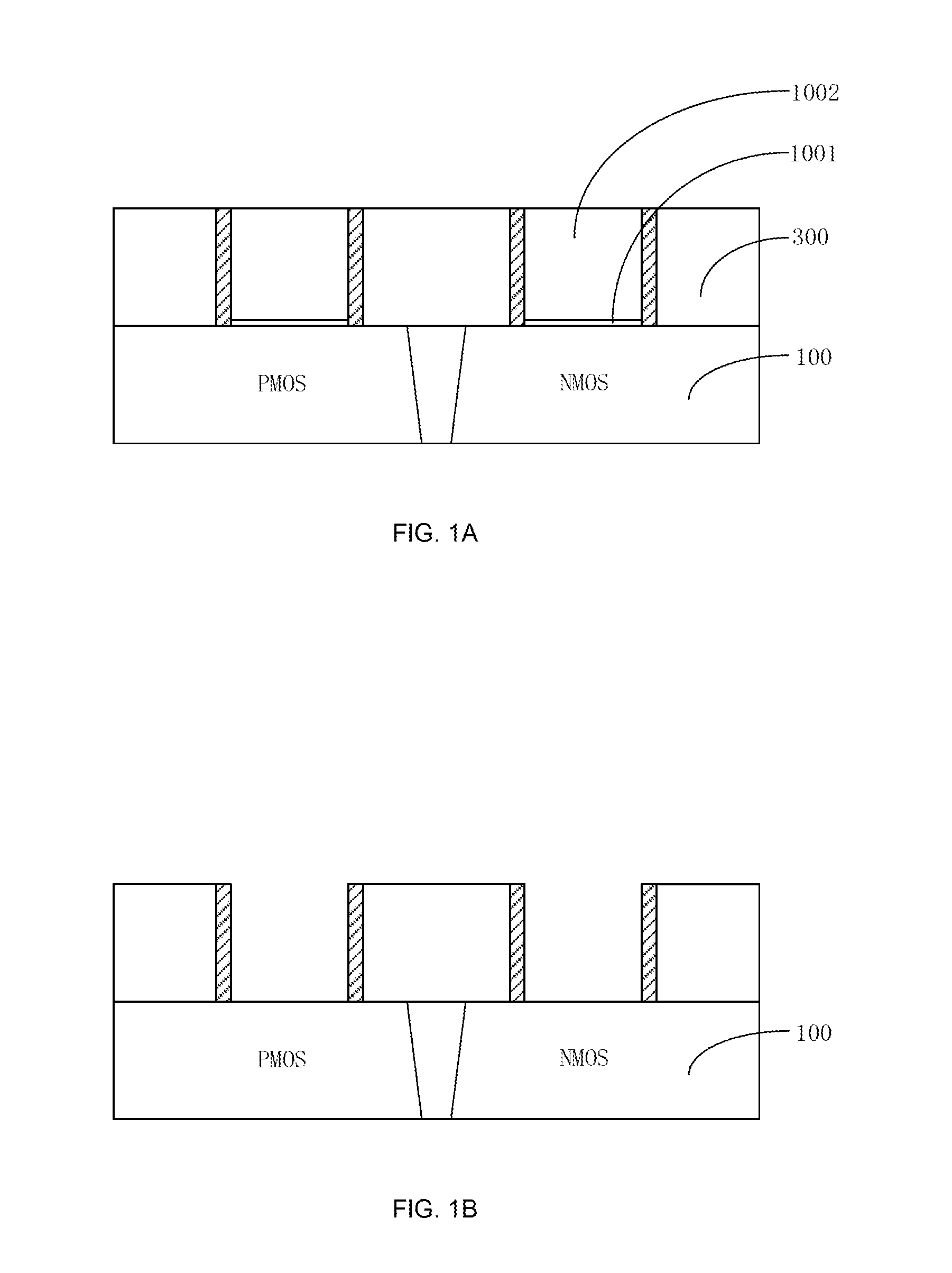
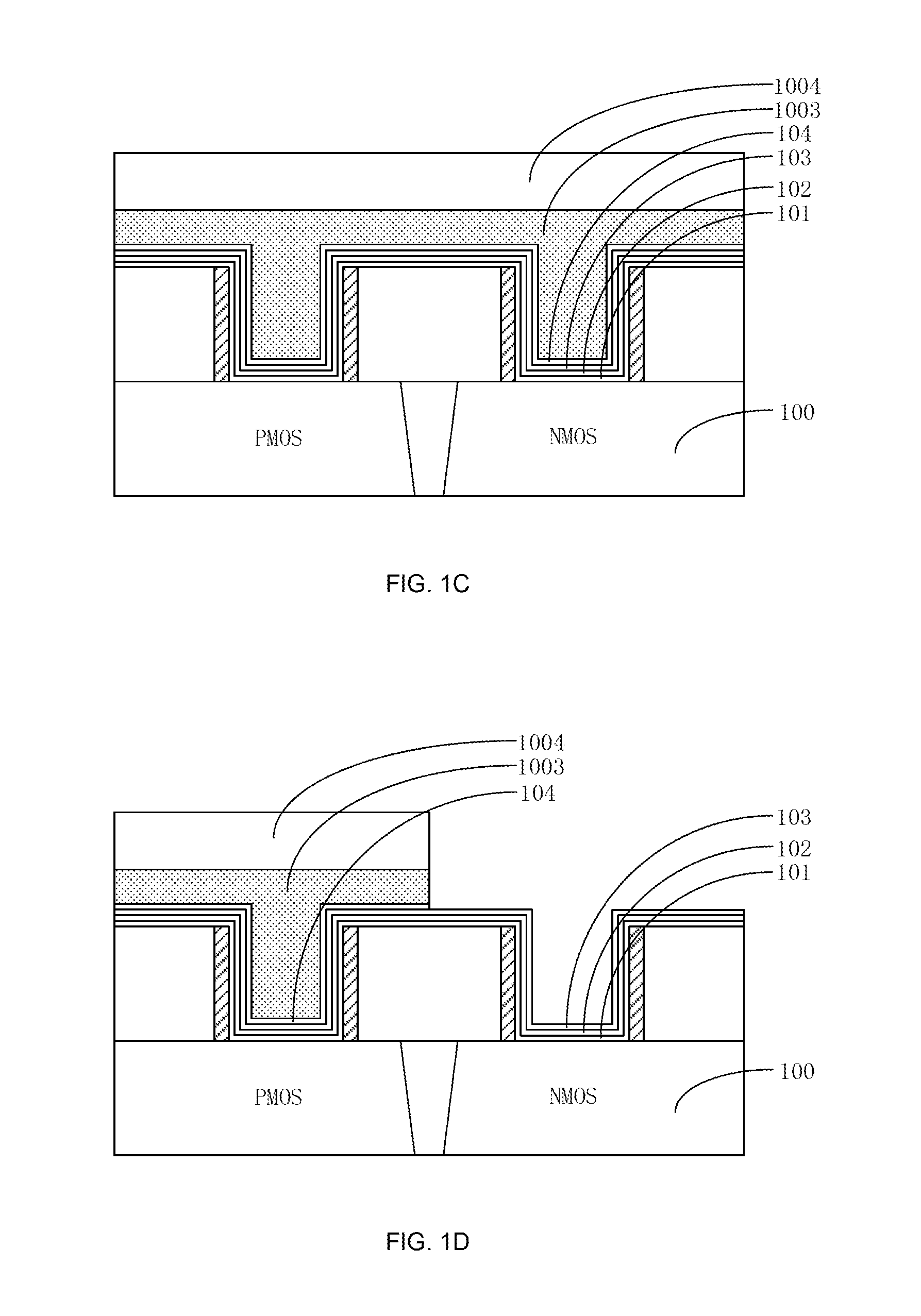
[0037]Example embodiments of the present invention are described with reference to the accompanying drawings. As those skilled in the art would realize, the described embodiments may be modified in various different ways, all without departing from the spirit or scope of the present invention. Embodiments of the present invention may be practiced without some or all of these specific details. Well known process steps and / or structures may not have been described in detail in order to not unnecessarily obscure the present invention.

[0038]The drawings and description are illustrative and not restrictive. Like reference numerals may designate like (e.g., analogous or identical) elements in the specification. Repetition of description may be avoided.

[0039]The relative sizes and thicknesses of elements shown in the drawings are for facilitate description and understanding, without limiting the present invention. In the drawings, the thicknesses of some layers, films, panels, regions, etc...


PUM


Abstract

A method for manufacturing a semiconductor device may include the following steps: preparing a substrate having a PMOS region and an NMOS; forming a first gate trench on the PMOS region; forming a first high-k dielectric layer and a first high-k cap layer that cover a bottom and sides of the first gate trench; forming a second gate trench on the NMOS region; forming a second high-k dielectric layer and a second high-k cap layer that cover a bottom and sides of the second gate trench; removing a portion of the first high-k dielectric layer and a portion of the first high-k cap layer that are positioned on a side of the first gate trench; and removing a portion of the second high-k dielectric layer and a portion of the second high-k cap layer that are positioned on a side of the second gate trench.

Description

CROSS-REFERENCE TO RELATED APPLICATION[0001]This application claims priority to and benefit of Chinese Patent Application No. 201410060803.6, filed on 21 Feb. 2014, the Chinese Patent Application being incorporated herein by reference in its entirety.BACKGROUND OF THE INVENTION[0002]The present invention is related to a method for manufacturing a semiconductor device.[0003]In semiconductor device manufacturing, for minimizing the size of a semiconductor device, a metal gate electrode (or metal gate) may be used instead of a traditional polysilicon gate electrode (or polysilicon gate). The metal gate may prevent issues related to polysilicon gate depletion and may minimize a threshold voltage associated with the semiconductor device.[0004]Typically, a metal gate may be implemented using one of the following methods: a high-k first, metal-gate first method; a high-k first, metal-gate last method; and a high-k last, metal-gate last method. For manufacturing a complementary metal-oxide-...

Claims


Application Information

Patent Timeline
Patent Type & Authority Applications(United States)
IPC IPC(8): H01L21/8238H01L29/423H01L29/51H01L21/311H01L29/66
CPCH01L29/66545H01L29/513H01L29/517H01L29/518H01L21/31116H01L29/512H01L21/823842H01L21/823857H01L29/42364H01L21/31144H01L21/32139
Inventor ZHAO, JIE
Owner SEMICON MFG INT (SHANGHAI) CORP
Why Eureka
Try Eureka