Wire bonding method for a semiconductor package

a wire bonding and semiconductor technology, applied in the direction of semiconductor/solid-state device manufacturing, electric devices, solid-state devices, etc., can solve the problems of inferior wire bond connection, reduced bonding yield, and conventional wire bonding method

Inactive Publication Date: 2003-10-23
AMKOR TECH SINGAPORE HLDG PTE LTD
View PDF68 Cites 20 Cited by
  • Summary
  • Abstract
  • Description
  • Claims
  • Application Information

AI Technical Summary

Problems solved by technology

However, this conventional wire bonding method, and the resulting semiconductor packages, suffer from defects due to the fact that conductive balls 8d are formed in advance on some of the input and output pads of the first semiconductor chip 2, afterwhich an end of a wire 8a is bonded to each of the balls 8d.
This can lead to an inferior wire bond connection, and reduced bonding yield.
Furthermore, because a separate process for forming the conductive balls 8d is required, wire bonding time is lengthened and the manufacturing cost of the entire semiconductor package is increased.

Method used


Image

  • Wire bonding method for a semiconductor package
  • Wire bonding method for a semiconductor package
  • Wire bonding method for a semiconductor package

Examples


Embodiment Construction

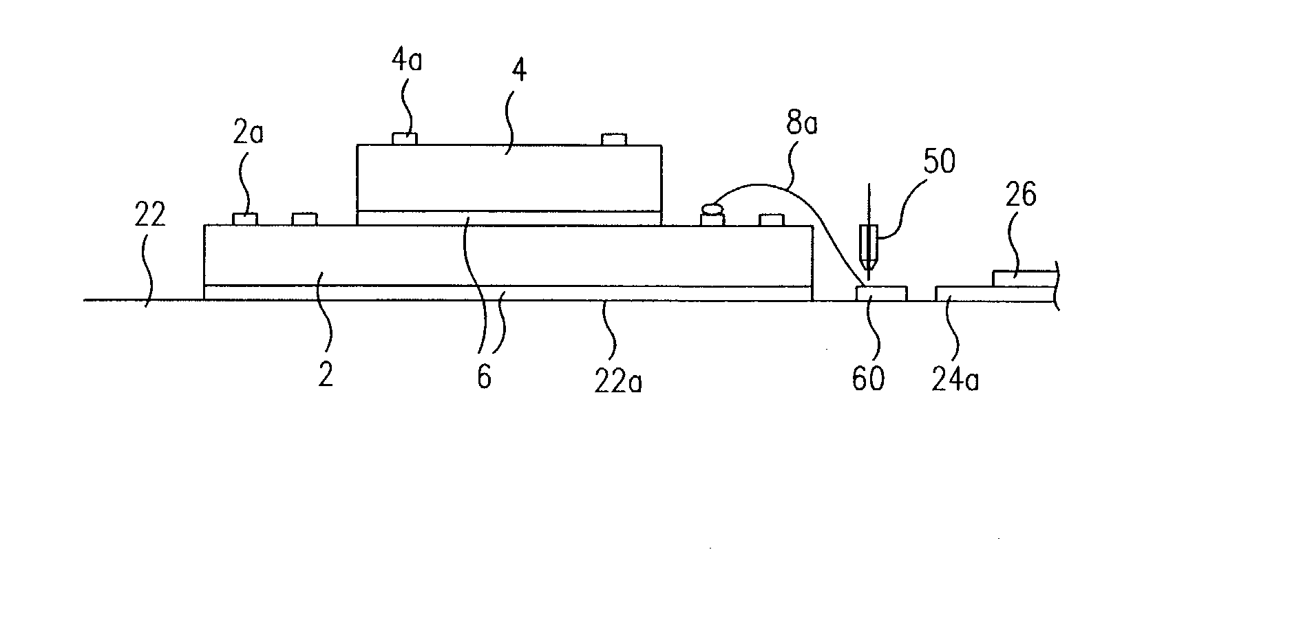
[0042] Reference will now be made in greater detail to exemplary embodiments of the invention. Wherever possible, the same reference numerals will be used throughout the drawings and the description to refer to the same or like parts.

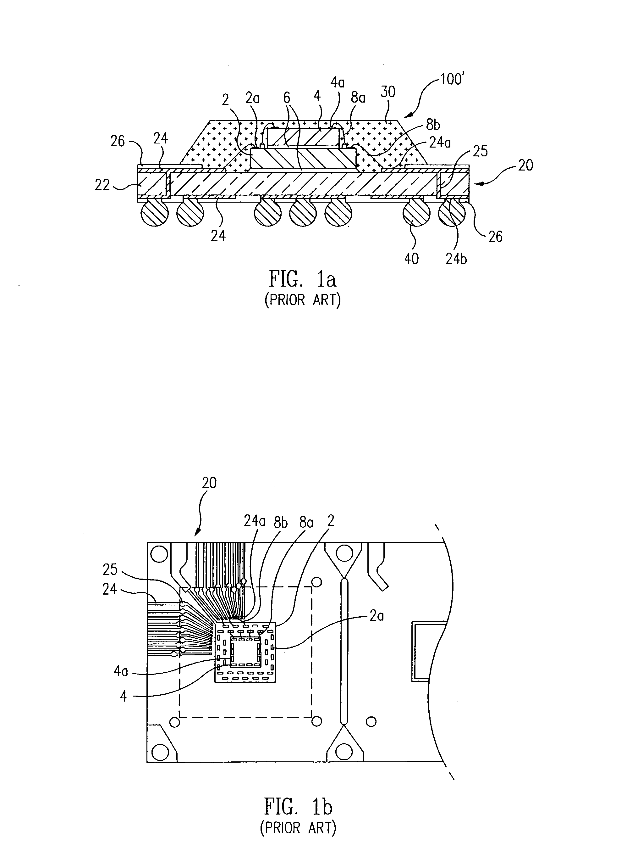
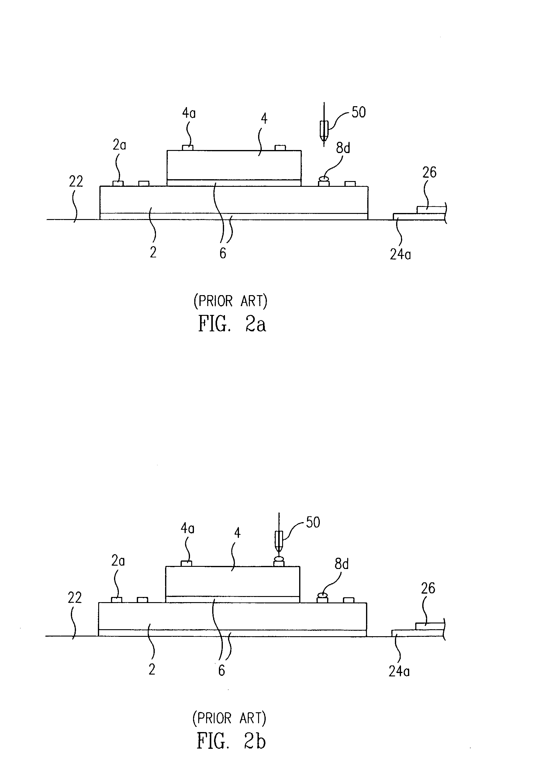
[0043] First, a planar circuit board 20 is provided (FIGS. 3a and 4). The circuit board 20 has a resin layer 22. A chip mounting region 22a is defined at a center portion of a planar upper surface of the resin layer 22. A plurality of circuit patterns 24, which include bond fingers 24a, are formed outside the chip mounting region 22a. Conductive transfer patterns 60 are formed on the upper surface of resin layer 22 laterally between the chip mounting region 22a and the circuit patterns 24.

[0044] A plurality of semiconductor chips are mounted on the upper surface of circuit board 20 within chip mounting region 22a.

[0045] In this embodiment, a first semiconductor chip 2 is affixed to the upper surface of resin layer 22 within chip mounting region 22a by a...


PUM


Abstract

A wire bonding method for electrically interconnecting stacked semiconductor chips is disclosed. A substrate (e.g., printed circuit board or metal leadframe) is provided. Metal circuit patterns are provided outside of a chip mounting region of the substrate, and metal transfer patterns are provided proximate to the chip mounting region. Stacked semiconductor are disposed in the chip mounting region. Conductive wires are bonded between respective pads of one stacked chip and respective transfer patterns, and other conductive wires are bonded between respective pads of the other stacked chip and the same respective transfer patterns, thereby electrically connecting respective pads of the two chips through a pair of bond wires and an intermediate transfer pattern. The transfer patterns are separate from circuit patterns of the substrate. At least one of the first and second chips is electrically connected to some of the circuit patterns for external connection.

Description

[0001] This application claims priority to U.S. patent application Ser. No. 09 / 745,265, filed Dec. 20, 2000 entitled "WIRE BONDING METHOD AND SEMICONDUCTOR PACKAGE MANUFACTURED USING THE SAME", and to Korean patent application serial number 1999-59329, which was filed with the Korean Intellectual Property Office on Dec. 20, 1999, both of which are incorporated herein by reference in their respective entireties.[0002] 1. Field of the Invention[0003] The present invention relates to a wire bonding method and a semiconductor package manufactured using the method, and, more particularly, the present invention relates to a wire bonding method and semiconductor package including a plurality of electrically interconnected semiconductor chips.[0004] 2. Description of the Related Art[0005] Conventionally, a semiconductor package may include a plurality of semiconductor chips that are stacked or arranged side by side on a printed circuit board, a lead frame or a circuit film. (The description...

Claims


Application Information

Patent Timeline
Patent Type & Authority Applications(United States)
IPC IPC(8): H01L21/60H01L23/31H01L25/065H01L25/18H01L25/07
CPCH01L23/3128H01L24/49H01L24/85H01L25/0655H01L25/0657H01L2224/32145H01L2224/32225H01L2224/48091H01L2224/48145H01L2224/48227H01L2224/48465H01L2224/4847H01L2224/48479H01L2224/4848H01L2224/49113H01L2224/73265H01L2224/78301H01L2224/85051H01L2224/85181H01L2224/92247H01L2225/06506H01L2225/0651H01L2225/06527H01L2225/06582H01L2225/06586H01L2924/01004H01L2924/01028H01L2924/01029H01L2924/01046H01L2924/01047H01L2924/01079H01L2924/01082H01L2924/15311H01L2924/19041H01L2924/19042H01L2924/19043H01L24/78H01L24/48H01L2924/014H01L2924/01033H01L2924/00014H01L2924/00H01L2224/451H01L2924/181H01L24/45H01L2224/05553H01L2224/45099H01L2924/00012H01L2224/4554H01L21/60
Inventor PARK, YOUNG KUKHAN, BYUNG JOONKIM, JAE DONG
Owner AMKOR TECH SINGAPORE HLDG PTE LTD
Why Eureka
Try Eureka