Partially Patterned Lead Frames and Methods of Making and Using the Same in Semiconductor Packaging

a technology of lead frame and patterned frame, which is applied in the field of semiconductor packaging, can solve the problems of handling flaws, affecting the finger-like portions of the lead frame are quite flimsy and difficult to hold in position, so as to facilitate the adhesion of the encapsulant, improve the retention of the encapsulant, and increase the surface area

Active Publication Date: 2007-03-08
UNISEM M BERHAD
View PDF53 Cites 109 Cited by
  • Summary
  • Abstract
  • Description
  • Claims
  • Application Information

AI Technical Summary

Benefits of technology

[0034] In addition to providing alterations for improved retention of the encapsulant, the surface of the lead frame may be roughened to provide for an increased surface area. The roughened surface will facilitate adhesion of the encapsulant to the surface of the lead frame.
[0035] A clip can optionally be used in place of wire bonding to increase the flow of power to the chip and thereby improve the performance of the chip.
[0036] It will be apparent from the above that the partially etched lead frame provides unity of structure and the attendant rigidity and strength to withstand the stress and strain of various manufacturing processes in the making of electronic packages. It is because of these unique mechanical properties that a partially etched lead frame package can also withstand connection to the next level of packaging, which previously has not been possible with conventional plastic packages.

Problems solved by technology

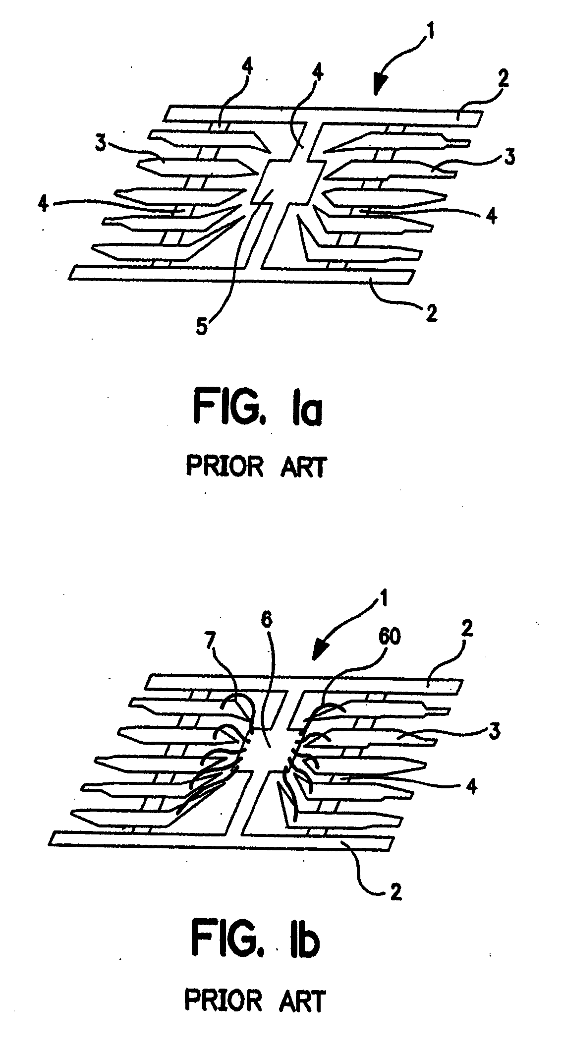
Conventional lead frames generally lack structural rigidity.
The finger-like portions of lead frames can be quite flimsy and difficult to hold in position.
This leads to handling flaws, damage and distortion in assembly processes and complicated wire bonding situations.
A failure to optimize the bonding parameters to compensate for the mechanical instability of the lead frame can result in poor bond adhesion, and hence poor quality and poor reliability of the bond.
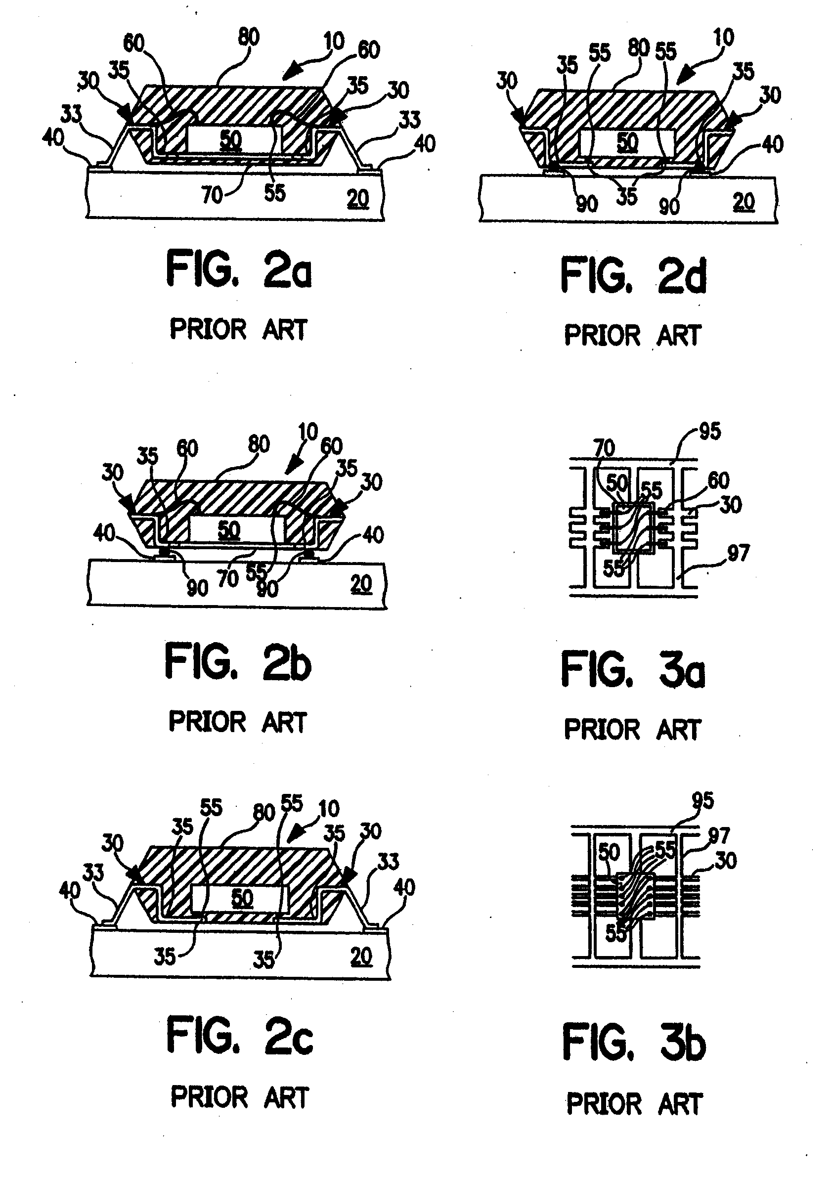
The prior art has not shown any lead frames that can withstand the stresses encountered in current semiconductor packaging processes and that can be manufactures in a cost effective manner.

Method used


Image

  • Partially Patterned Lead Frames and Methods of Making and Using the Same in Semiconductor Packaging
  • Partially Patterned Lead Frames and Methods of Making and Using the Same in Semiconductor Packaging
  • Partially Patterned Lead Frames and Methods of Making and Using the Same in Semiconductor Packaging

Examples


Embodiment Construction

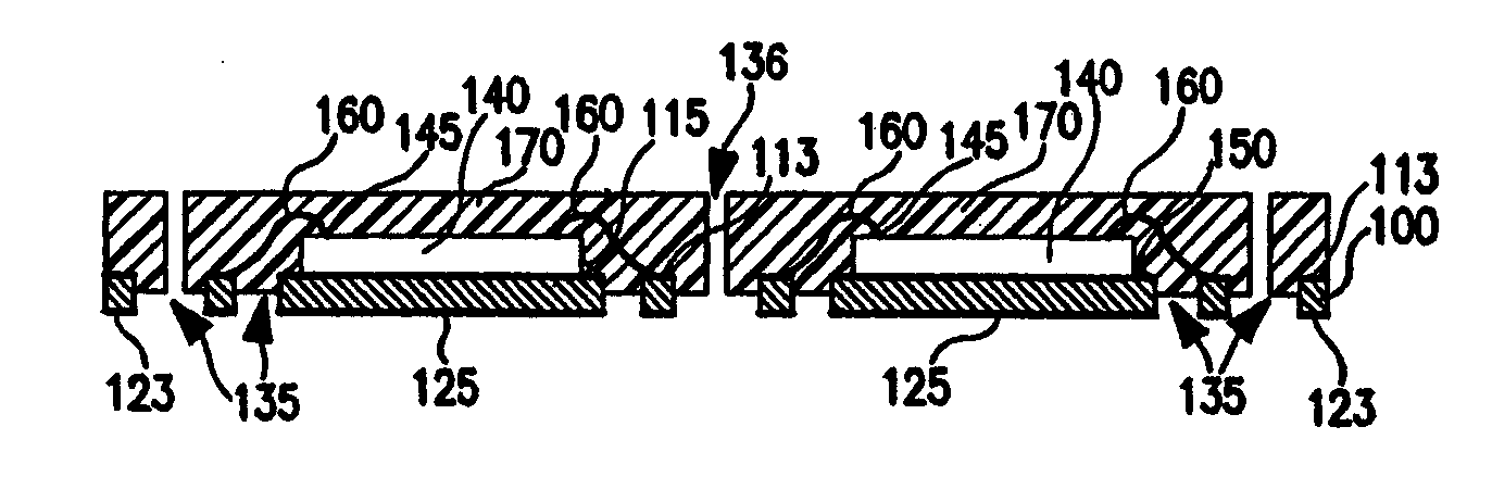
[0082] The present invention will now be described with reference to the Figures, wherein like numeral refer to like elements. FIGS. 4-15b and FIGS. 16-24b show different embodiments of forming a partially patterned lead frame package with lead counts comparable to that of near-chip scale packages (CSPs). The method of the invention improves the automation of the manufacturing line and the quality and reliability of the packages made therefrom. This is accomplished by performing a major portion of the manufacturing process steps with a partially patterned metal film formed into a web-like lead frame on one side. In contrast with conventionally punched through stencil-like lead frames, the lead frame used in the invention is partially patterned on one side and is solid and flat on the other side. This construction is improved both mechanically and thermally, and performs without distortion or deformation during the chip-attach, wire bond, and encapsulation processes. After the chip a...


PUM


Abstract

A method of making a lead frame and a partially patterned lead frame package with near-chip scale packaging (CSP) lead-counts is disclosed, wherein the method lends itself to better automation of the manufacturing line as well as to improving the quality and reliability of the packages produced therefrom. This is accomplished by performing a major portion of the manufacturing process steps with a partially patterned strip of metal formed into a web-like lead frame on one side, in contrast with the conventional fully etched stencil-like lead frames, so that the web-like lead frame, which is solid and flat on the other side is also rigid mechanically and robust thermally to perform without distortion or deformation during the chip-attach and wire bond processes, both at the chip level and the package level. The bottom side of the metal lead frame is patterned to isolate the chip-pad and the wire bond contacts only after the front side, including the chip and wires, is hermetically sealed with an encapsulant. The resultant package being electrically isolated enables strip testing and reliable singulation without having to cut into any additional metal. The use of the instant partially patterned lead frame in making ELP, ELPF and ELGA-type CSPs is also disclosed.

Description

[0001] This application is a continuation-in-part of both (a) application Ser. No. 11 / 197,944, filed Aug. 4, 2005, which is a continuation of application Ser. No. 10 / 916,093, filed Aug. 10, 2004; and (b) the aforementioned application Ser. No. 10 / 916,093. application Ser. No. 10 / 916,093 is a continuation of application Ser. No. 10 / 134,882, filed Apr. 29, 2002, now U.S. Pat. No. 6,812,552. All of these applications are incorporated herein by reference in their entirety.FIELD OF THE INVENTION [0002] The invention relates to electronic packaging in general, and more particularly, to a partially patterned lead frame and a method for making and using the same. The partially patterned lead frame is stronger and more stable than conventional lead frames. The sturdiness of the partially patterned lead frame improves the process of manufacturing lead frame packages and enhances the overall reliability of the end product. The lead frame also offers a high degree of flexibility for device inte...

Claims


Application Information

Patent Timeline
Patent Type & Authority Applications(United States)
IPC IPC(8): H01L23/495H01L21/00
CPCH01L21/4832H01L21/561H01L23/49524H01L23/49548H01L24/45H01L24/49H01L24/73H01L24/97H01L2221/68377H01L2224/32145H01L2224/32245H01L2224/45124H01L2224/45147H01L2224/48091H01L2224/48145H01L2224/48247H01L2224/49171H01L2224/73221H01L2224/73265H01L2224/85205H01L2224/92247H01L2224/97H01L2225/06568H01L2924/01005H01L2924/01013H01L2924/01028H01L2924/01029H01L2924/01046H01L2924/01047H01L2924/0105H01L2924/01075H01L2924/01078H01L2924/01079H01L2924/01082H01L2924/14H01L2924/15311H01L2924/19041H01L2924/19043H01L2924/19105H01L24/48H01L2224/16245H01L2224/48257H01L2924/01006H01L2924/01033H01L2924/014H01L2924/07802H01L2924/00014H01L2224/85H01L2224/81H01L2924/00012H01L2224/83H01L2924/00H01L2224/45015H01L2924/351H01L2924/181H01L2224/45014H01L2224/78744H01L2924/20759H01L2924/2076H01L2924/20752H01L2924/20753H01L2924/20755H01L2924/20756H01L2924/20757H01L2924/20758H01L2924/2075H01L2924/20754H01L2924/206
Inventor RAMOS, MARY JEANSAN ANTONIO, ROMARICO SANTOSSUBAGIO, ANANG
Owner UNISEM M BERHAD
Why Eureka
Try Eureka