Quad flat no-lead chip carrier

a chip carrier and flat no-lead technology, applied in the field of chip carriers, can solve problems such as the quality of the chip package may be affected, and achieve the effects of improving the overall quality of the chip package, reducing the distance between two neighboring conductive columns, and increasing the density of i/o contacts within the chip packag

Active Publication Date: 2005-04-19
VIA TECH INC
View PDF3 Cites 108 Cited by
  • Summary
  • Abstract
  • Description
  • Claims
  • Application Information

AI Technical Summary

Benefits of technology

[0013]This invention deploys a conductive plate with a plurality of columnar through holes to serve as the carrier of a chip. The chip is electrically connected to the conductive column within each columnar through hole in the conductive plate. Furthermore, the conductive column forms various independent input/output (I/O) contacts through the insulating effect of dielectric walls. Because the distance of separation between two neighboring conducti

Problems solved by technology

Since the bled out insulating material 150 is hard to

Method used


Image

  • Quad flat no-lead chip carrier
  • Quad flat no-lead chip carrier
  • Quad flat no-lead chip carrier

Examples


Embodiment Construction

[0021]Reference will now be made in detail to the present preferred embodiments of the invention, examples of which are illustrated in the accompanying drawings. Wherever possible, the same reference numbers are used in the drawings and the description to refer to the same or like parts.

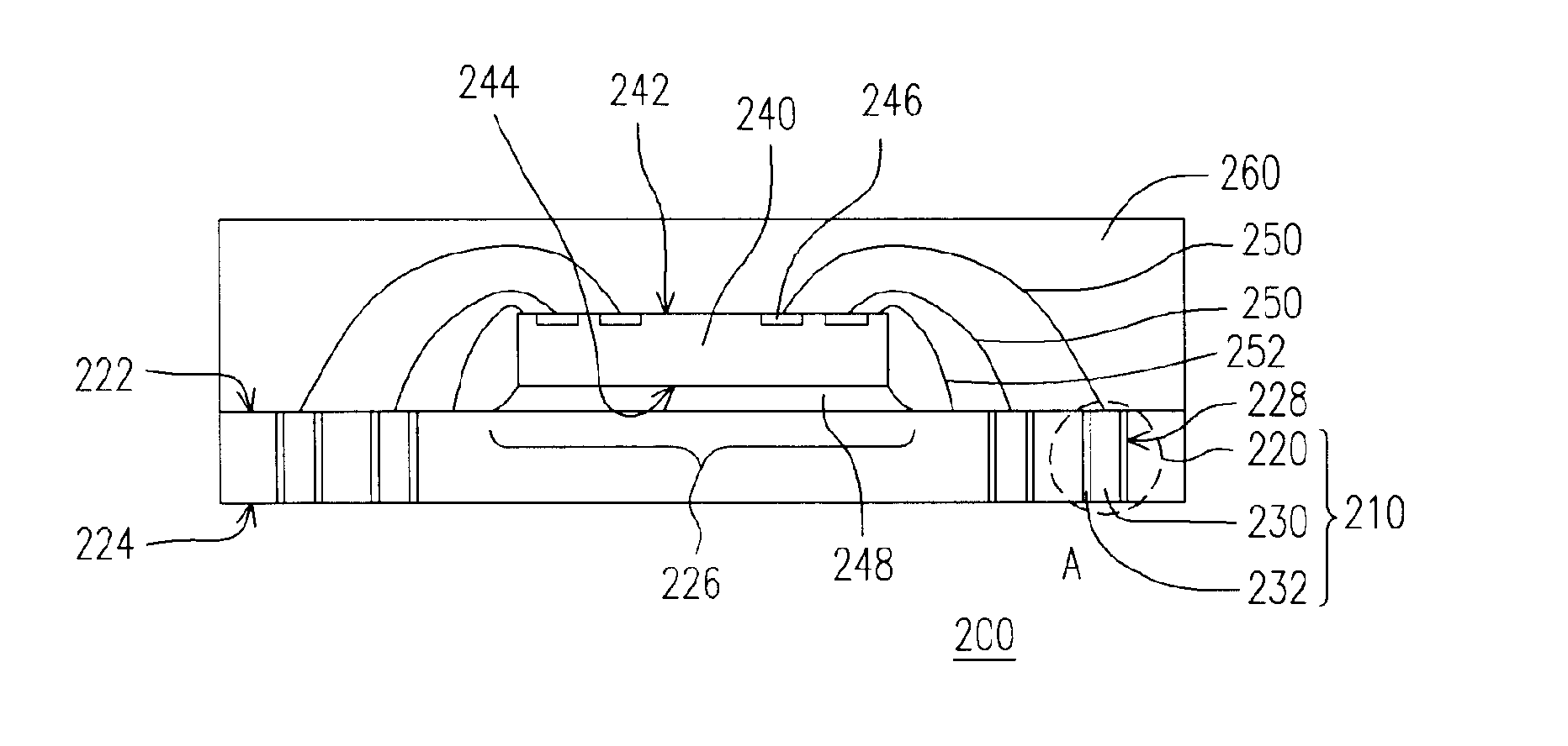
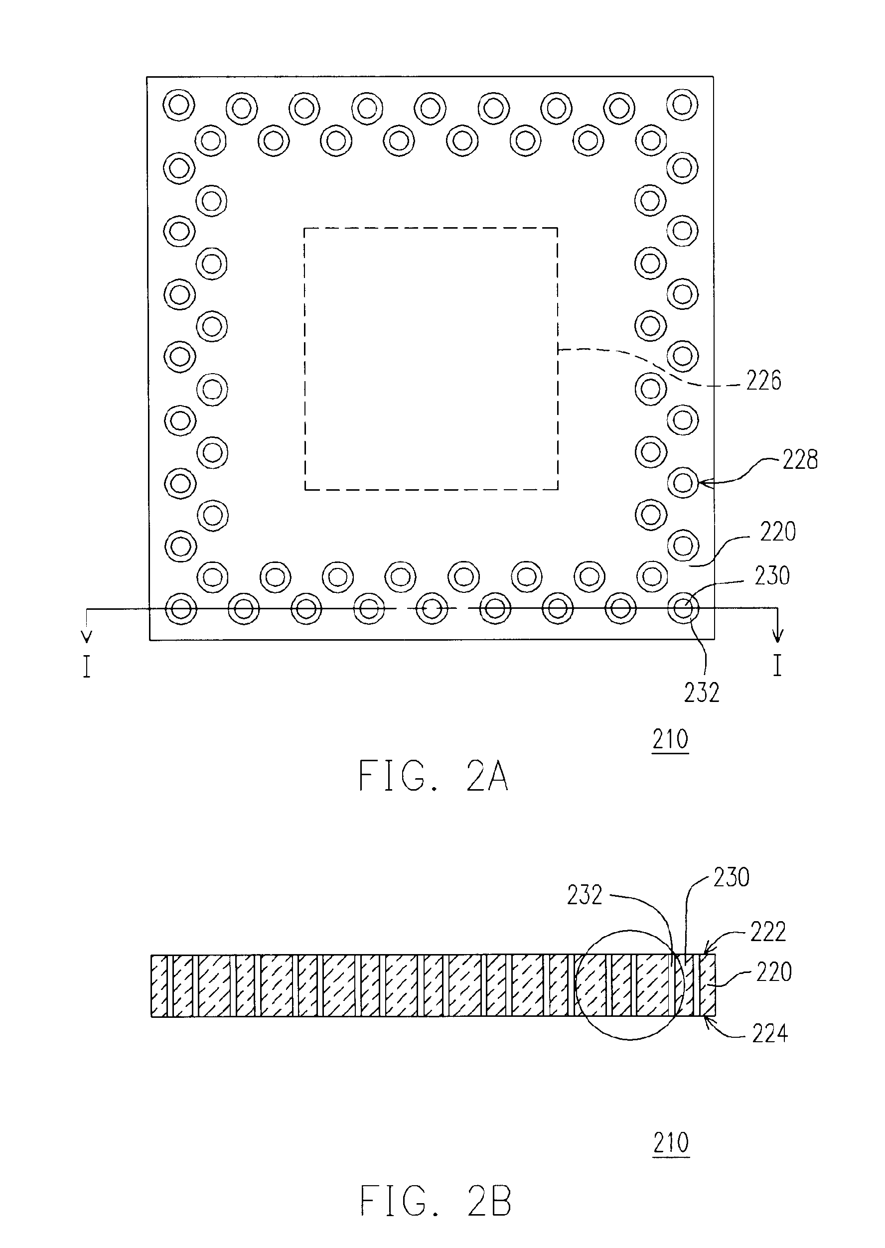
[0022]FIG. 2A is a top view showing a quad flat no-lead type of chip carrier according to one preferred embodiment of this invention. FIG. 2B is a cross-sectional view along line 1—1 in FIG. 2A. As shown in FIG. 2A, the chip carrier 210 comprises a conductive plate 220, a plurality of conductive columns 230 and a plurality of dielectric walls 232. The conductive plate 220 has a first surface 222 and a second surface 224. The first surface 222 has a chip-bonding region 226. The conductive plate 220 further has a plurality of surrounding columnar through holes 228 which are distributed on the periphery of the chip-bonding region 226. Each columnar through hole 228 passes through the conductive plate 22...


PUM


Abstract

A quad flat no-lead chip carrier for a wire-bonded chip package is provided. The chip carrier comprises a conductive plate, a plurality of conductive columns and a plurality of dielectric walls. A chip is attached to the conductive plate. The conductive plate furthermore has a plurality of columnar through holes distributed around a chip-bonding region. The conductive columns are set up within the columnar through holes. The dielectric walls are set up between the sidewall of the conductive columns and the inner surface of the columnar through holes. The chip is electrically connected to the conductive columns via conductive wires. The bottom end of the conductive columns serves as input/output contacts for connecting with external contacts. The chip carrier is able to increase overall density of the input/output contacts and improve the electrical performance of the chip package.

Description

CROSS REFERENCE TO RELATED APPLICATIONS[0001]This application claims the priority benefit of Taiwan application serial no. 92117230, filed on Jun. 25, 2003.BACKGROUND OF INVENTION[0002]1. Field of Invention[0003]The present invention relates to a chip carrier. More particularly, the present invention relates to a quad flat no-lead (QFN) chip carrier and a chip package structure.[0004]2. Description of Related Art[0005]Semiconductor fabrication is a most rapidly developed high-tech industry. Following recent advance in electronic technologies, many types of personalized and multi-functional electronic products with a compact design are out in the market. At present, lead frame is still one of the major components in packaging semiconductor chips. According to the type of leads in the lead frame, a quad flat package (QFP) can be divided into quad flat package with I-type leads (QFI), quad flat package with J-type leads (QFJ) and quad flat package no-lead (QFN). Because the outer end o...

Claims


Application Information

Patent Timeline
IPC IPC(8): H01L23/31H01L23/28H01L23/492H01L23/498H01L23/48
CPCH01L23/3121H01L23/49827H01L24/49H01L23/492H01L24/48H01L2224/48091H01L2224/48227H01L2224/48235H01L2224/48247H01L2224/48257H01L2224/49H01L2224/73265H01L2924/01013H01L2924/01029H01L2924/01047H01L2924/01082H01L2924/3025H01L2924/014H01L2924/01033H01L2224/32245H01L2924/00014H01L2924/00H01L2924/00012H01L24/73H01L2924/181H01L2224/45099H01L2224/05599
Inventor HSU, CHI-HSING
Owner VIA TECH INC
Why Eureka
Try Eureka