Manufacturing method for rewiring quad flat no-lead (QFN) packaging component

A technology for packaging devices and manufacturing methods, which is applied in semiconductor/solid-state device manufacturing, electric solid-state devices, semiconductor devices, etc., can solve problems that affect the yield and reliability of packaging devices, metal wire collapse, increase manufacturing costs, etc., and achieve improvement Yield and reliability, low cost, effect of solving collapse

Inactive Publication Date: 2015-05-13
BEIJING UNIV OF TECH
View PDF3 Cites 0 Cited by
  • Summary
  • Abstract
  • Description
  • Claims
  • Application Information

AI Technical Summary

Problems solved by technology

However, in order to increase the number of I / Os of QFN packaged devices, more areas are needed to place multiple pins, so the size of QFN packaged devices needs to be increased, which is contrary to the requirements of miniaturization of packaged devices, and with the package As the size increases, the distance between the chip and the pins will increase, resulting in an increase in the use of metal wires, such as gold (Au) wires, which increases manufacturing costs. Too long metal wires can easily cause metal wires during the injection molding process. Problems such as collapse, line punching, and crossing lines affect the improvement of the yield and reliability of packaged devices
Therefore, in order to break through the oversized bottleneck of the existing multi-turn pin arrangement QFN package device, solve the above-mentioned yield and reliability problems and reduce manufacturing costs, it is urgent to develop a small size, high reliability, low cost, high QFN package device with I / O density and manufacturing method thereof

Method used


Image

  • Manufacturing method for rewiring quad flat no-lead (QFN) packaging component
  • Manufacturing method for rewiring quad flat no-lead (QFN) packaging component
  • Manufacturing method for rewiring quad flat no-lead (QFN) packaging component

Examples


Embodiment Construction

[0045] The present invention is described in detail below in conjunction with accompanying drawing:

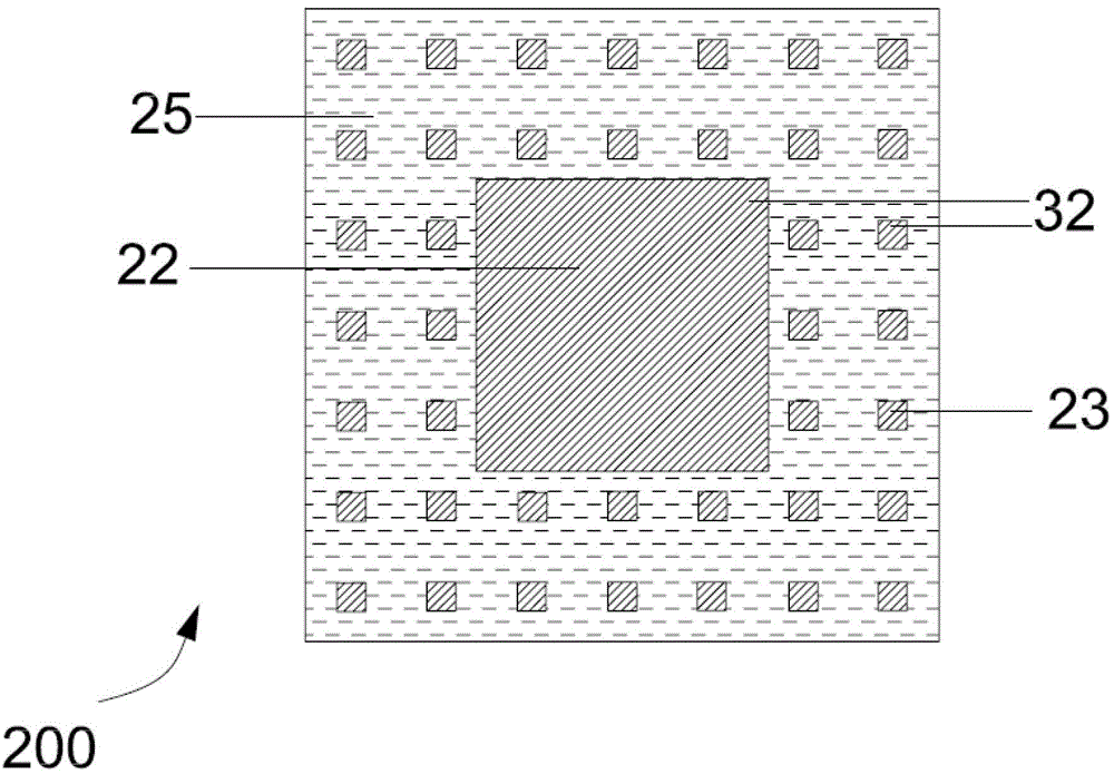
[0046] Figure 2A A schematic diagram of the rear side of a rewiring QFN packaged device in which the cross-section of the pins is rectangular and the pins on each side of the chip carrier are arranged in parallel according to the embodiment of the present invention.

[0047] Refer to the above Figure 2A It can be seen that, in this embodiment, the rewiring QFN packaged device 200 has a chip carrier 22 and pins 23 arranged in two circles around the chip carrier 22, and the pins 23 on each side of the chip carrier 22 are arranged in parallel, The cross section of the lead 23 is rectangular, the second metal material layer 32 is arranged on the lower surface of the chip carrier 22 and the lead 23 , and the insulating filling material 25 is arranged in the redistribution QFN package device 200 . In this embodiment, the number of arrangement turns of the pins 23 is not limited, i...


PUM


Abstract

The invention discloses a manufacturing method for a rewiring quad flat no-lead (QFN) packaging component. A chip carrier and lead feet of the manufactured rewiring QFN packaging component are formed by using of an etching method in the process of packaging technology. Insulating filling materials are arranged between the chip carrier and the lead feet, and in grooves between the lead feet by using an injection molding method or a silk-screen printing method. Rewiring layers are manufactured by using of electroplating and chemical plating methods and are packaged by using of plastic package materials. After the process of plastic package, an independent chip carrier and independent lead feet are formed by using of the etching method or a mechanical grinding method. The manufactured rewiring QFN packaging component is high in input / output (I / O) density, low in manufacturing cost and good in reliability.

Description

technical field [0001] The invention relates to the technical field of manufacturing QFN components, in particular to a quadrilateral flat no-lead package with high I / O density and a manufacturing method thereof. Background technique [0002] With the development of electronic products such as mobile phones and notebook computers towards miniaturization, portability, ultra-thinness, multimedia and low-cost requirements for popularization, high-density, high-performance, high-reliability and low-cost packaging forms and Its assembly technology has been developed rapidly. Compared with expensive BGA and other packaging forms, the new packaging technology developed rapidly in recent years, that is, Quad Flat Non-lead Package (QFN) package, has good thermal and electrical properties, small size, Many advantages such as low cost and high productivity have triggered a new revolution in the field of microelectronic packaging technology. [0003] Due to the improvement of IC integ...

Claims


Application Information

Patent Timeline
Patent Type & Authority Patents(China)
IPC IPC(8): H01L21/48H01L21/56H01L21/60
CPCH01L24/97H01L2224/32245H01L2224/48091H01L2224/48095H01L2224/48247H01L2224/49171H01L2224/73265H01L2224/92247H01L2224/97H01L2924/181
Inventor 秦飞夏国峰安彤刘程艳武伟朱文辉
Owner BEIJING UNIV OF TECH
Why Eureka
Try Eureka